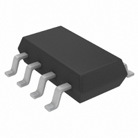
LT3008ITS8-1.5#TRMPBF Linear Technology, LT3008ITS8-1.5#TRMPBF Datasheet - Page 12

LT3008ITS8-1.5#TRMPBF
Manufacturer Part Number
LT3008ITS8-1.5#TRMPBF
Description
IC REG LDO 1.5V 20MA TSOT23-8
Manufacturer
Linear Technology
Datasheet
1.LT3008EDCTRMPBF.pdf
(20 pages)
Specifications of LT3008ITS8-1.5#TRMPBF
Regulator Topology
Positive Fixed
Voltage - Output
1.5V
Voltage - Input
2 ~ 45 V
Voltage - Dropout (typical)
0.3V @ 20mA
Number Of Regulators
1
Current - Output
20mA
Current - Limit (min)
22mA
Operating Temperature
-40°C ~ 125°C
Mounting Type
Surface Mount
Package / Case
TSOT-23-8, TSOT-8
Lead Free Status / RoHS Status
Lead free / RoHS Compliant
Available stocks
Company
Part Number
Manufacturer
Quantity
Price
The LT3008 is a low dropout linear regulator with ultra-
low quiescent current and shutdown. Quiescent current
is extremely low at 3μA and drops well below 1μA in
shutdown. The device supplies up to 20mA of output current.
Dropout voltage at 20mA is typically 300mV. The LT3008
incorporates several protection features, making it ideal for
use in battery-powered systems. The device protects itself
against both reverse-input and reverse-output voltages.
In battery backup applications, where a backup battery
holds up the output when the input is pulled to ground,
the LT3008 acts as if a blocking diode is in series with its
output and prevents reverse current fl ow. In applications
where the regulator load returns to a negative supply, the
output can be pulled below ground by as much as 50V
without affecting start-up or normal operation.
Adjustable Operation
The LT3008 has an output voltage range of 0.6V to 44.5V.
Figure 2 shows that output voltage is set by the ratio of two
external resistors. The IC regulates the output to maintain
the ADJ pin voltage at 600mV referenced to ground. The
current in R1 equals 600mV/R1 and the current in R2 is
the current in R1 minus the ADJ pin bias current. The ADJ
pin bias current, typically 400pA at 25°C, fl ows out of the
pin. Calculate the output voltage using the formula in Figure
2. An R1 value of 619k sets the divider current to 0.97μA.
Do not make R1’s value any greater than 619k to minimize
output voltage errors due to the ADJ pin bias current and
LT3008 Series
APPLICATIONS INFORMATION
12
V
V
I
OUTPUT RANGE = 0.6V to 44.5V
ADJ
OUT
ADJ
= 0.4nA at 25°C
= 600mV
= 600mV • (1 + R2/R1) – (I
ADJ
Figure 2. Adjustable Operation
• R2)
V
IN
Table 1. Output Voltage Resistor Divider Values
to insure stability under minimum load conditions. In
shutdown, the output turns off and the divider current is
zero. Curves of ADJ Pin Voltage vs Temperature and ADJ
Pin Bias Current vs Temperature appear in the Typical
Performance Characteristics.
Specifi cations for output voltages greater than 0.6V are
proportional to the ratio of the desired output voltage to
0.6V: V
current change of 100μA to 20mA is –0.5mV typical at
V
Table 1 shows resistor divider values for some com-
mon output voltages with a resistor divider current of
about 1μA.
OUT
0 6
5
.
IN
SHDN
= 0.6V. At V
V
OUT
V
V
1.2V
1.5V
1.8V
2.5V
3.3V
LT3008
1V
3V
5V
OUT
GND
• (
/0.6V. For example, load regulation for an output
−
OUT
ADJ
0 5
.
mV
OUT
R2
R1
)
= 5V, load regulation is:
= −
4 17
604k
590k
590k
590k
590k
590k
619k
590k
.
R1
V
3008 F02
OUT
mV
1.18M
1.87M
2.37M
4.32M
2.8M
402k
590k
887k
R2
3008fb


