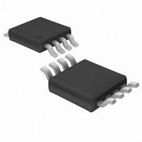
LT3020EMS8-1.2#TR Linear Technology, LT3020EMS8-1.2#TR Datasheet - Page 12

LT3020EMS8-1.2#TR
Manufacturer Part Number
LT3020EMS8-1.2#TR
Description
IC REG LDO 1.2V 100MA LV 8MSOP
Manufacturer
Linear Technology
Datasheet
1.LT3020EDDPBF.pdf
(16 pages)
Specifications of LT3020EMS8-1.2#TR
Regulator Topology
Positive Fixed
Voltage - Output
1.2V
Voltage - Input
Up to 10V
Voltage - Dropout (typical)
0.15V @ 100mA
Number Of Regulators
1
Current - Output
100mA
Current - Limit (min)
110mA
Operating Temperature
-40°C ~ 125°C
Mounting Type
Surface Mount
Package / Case
8-MSOP, Micro8™, 8-uMAX, 8-uSOP,
Lead Free Status / RoHS Status
Contains lead / RoHS non-compliant
Available stocks
Company
Part Number
Manufacturer
Quantity
Price
APPLICATIO S I FOR ATIO
LT3020/LT3020-1.2/
LT3020-1.5/LT3020-1.8
Table 2. Measured Thermal Resistance for MS8 Package
*Device is mounted on topside.
Calculating Junction Temperature
Example: Given an output voltage of 1.8V, an input voltage
range of 2.25V to 2.75V, an output current range of 1mA
to 100mA, and a maximum ambient temperature of 70°C,
what will the maximum junction temperature be for an
application using the DD package?
The power dissipated by the device is equal to:
where
so
The thermal resistance is in the range of 35°C/W to
70°C/W depending on the copper area. So the junction
temperature rise above ambient is approximately equal to:
The maximum junction temperature equals the maximum
junction temperature rise above ambient plus the maxi-
mum ambient temperature or:
Protection Features
The LT3020 incorporates several protection features that
make it ideal for use in battery-powered circuits. In addi-
tion to the normal protection features associated with
monolithic regulators, such as current limiting and ther-
mal limiting, the device also protects against reverse-
input voltages, reverse-output voltages and reverse
output-to-input voltages.
12
TOPSIDE*
2500mm
1000mm
225mm
100mm
I
I
V
I
P = 100mA(2.75V – 1.8V) + 3mA(2.75V) = 0.103W
0.103W(52.5°C/W) = 5.4°C
T
50mm
OUT(MAX)
OUT(MAX)
GND
JMAX
IN(MAX)
COPPER AREA
2
at (I
2
2
2
2
= 70°C + 5.4°C = 75.4°C
= 2.75V
OUT
BACKSIDE
(V
2500mm
2500mm
2500mm
2500mm
2500mm
= 100mA
IN(MAX)
= 100mA, V
U
2
2
2
2
2
– V
BOARD AREA (JUNCTION-TO-AMBIENT)
2500mm
2500mm
2500mm
2500mm
2500mm
U
OUT
IN
) + I
= 2.75V) = 3mA
2
2
2
2
2
GND
W
THERMAL RESISTANCE
(V
IN(MAX)
110°C/W
115°C/W
120°C/W
130°C/W
140°C/W
U
)
Current limit protection and thermal overload protection
protect the device against current overload conditions at
the output of the device. For normal operation, do not
exceed a junction temperature of 125°C.
The IN pins of the device withstand reverse voltages of
10V. The LT3020 limits current flow to less than 1µA and
no negative voltage appears at OUT. The device protects
both itself and the load against batteries that are plugged
in backwards.
The LT3020 incurs no damage if OUT is pulled below
ground. If IN is left open circuit or grounded, OUT can be
pulled below ground by 10V. No current flows from the
pass transistor connected to OUT. However, current flows
in (but is limited by) the resistor divider that sets the output
voltage. Current flows from the bottom resistor in the
divider and from the ADJ pin’s internal clamp through the
top resistor in the divider to the external circuitry pulling
OUT below ground. If IN is powered by a voltage source,
OUT sources current equal to its current limit capability
and the LT3020 protects itself by thermal limiting. In this
case, grounding SHDN turns off the LT3020 and stops
OUT from sourcing current.
The LT3020 incurs no damage if the ADJ pin is pulled
above or below ground by 10V. If IN is left open circuit or
grounded and ADJ is pulled above ground, ADJ acts like a
25k resistor in series with a 1V clamp (one Schottky diode
in series with one diode). ADJ acts like a 25k resistor in
series with a Schottky diode if pulled below ground. If IN
is powered by a voltage source and ADJ is pulled below its
reference voltage, the LT3020 attempts to source its
current limit capability at OUT. The output voltage in-
creases to V
load current the LT3020 supports. This condition can
potentially damage external circuitry powered by the
LT3020 if the output voltage increases to an unregulated
high voltage. If IN is powered by a voltage source and ADJ
is pulled above its reference voltage, two situations can
occur. If ADJ is pulled slightly above its reference voltage,
the LT3020 turns off the pass transistor, no output current
is sourced and the output voltage decreases to either the
voltage at ADJ or less. If ADJ is pulled above its no load
recovery threshold, the no load recovery circuitry turns on
and attempts to sink current. OUT is actively pulled low
IN
– V
DROPOUT
with V
DROPOUT
set by whatever
3020fc


