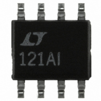
LT1121AIS8 Linear Technology, LT1121AIS8 Datasheet - Page 9

LT1121AIS8
Manufacturer Part Number
LT1121AIS8
Description
IC REG LDO ADJ 150MA 8-SOIC
Manufacturer
Linear Technology
Datasheet
1.LT1121CZ-5PBF.pdf
(16 pages)
Specifications of LT1121AIS8
Regulator Topology
Positive Adjustable
Voltage - Output
3.75 ~ 30 V
Voltage - Input
4.17 ~ 30 V
Voltage - Dropout (typical)
0.42V @ 150mA
Number Of Regulators
1
Current - Output
150mA
Operating Temperature
-40°C ~ 125°C
Mounting Type
Surface Mount
Package / Case
8-SOIC (3.9mm Width)
Lead Free Status / RoHS Status
Contains lead / RoHS non-compliant
Current - Limit (min)
-
Available stocks
Company
Part Number
Manufacturer
Quantity
Price
Company:
Part Number:
LT1121AIS8
Manufacturer:
LT
Quantity:
10 000
Part Number:
LT1121AIS8
Manufacturer:
LINEAR/凌特
Quantity:
20 000
Company:
Part Number:
LT1121AIS8#TRPBF
Manufacturer:
LT
Quantity:
4 200
Company:
Part Number:
LT1121AIS8-3.3
Manufacturer:
LT
Quantity:
10 000
Part Number:
LT1121AIS8-3.3
Manufacturer:
LINEAR/凌特
Quantity:
20 000
Company:
Part Number:
LT1121AIS8-3.3#TRPBF
Manufacturer:
SEMELAB
Quantity:
76
Part Number:
LT1121AIS8-5
Manufacturer:
LT
Quantity:
20 000
Company:
Part Number:
LT1121AIS8-5#TRPBF
Manufacturer:
LT
Quantity:
3 940
APPLICATIONS INFORMATION
The LT1121 is a micropower low dropout regulator with
shutdown, capable of supplying up to 150mA of output
current at a dropout voltage of 0.4V. The device operates
with very low quiescent current (30μA). In shutdown the
quiescent current drops to only 16μA. In addition to the
low quiescent current the LT1121 incorporates several
protection features which make it ideal for use in bat-
tery-powered systems. The device is protected against
both reverse input voltages and reverse output voltages.
In battery backup applications where the output can be
held up by a backup battery when the input is pulled to
ground, the LT1121 acts like it has a diode in series with
its output and prevents reverse current fl ow.
Adjustable Operation
The adjustable version of the LT1121 has an output voltage
range of 3.75V to 30V. The output voltage is set by the
ratio of two external resistors as shown in Figure 1. The
device servos the output voltage to maintain the voltage
at the adjust pin at 3.75V. The current in R1 is then equal
to 3.75V/R1. The current in R2 is equal to the sum of the
current in R1 and the adjust pin bias current. The adjust
pin bias current, 150nA at 25°C, fl ows through R2 into the
adjust pin. The output voltage can be calculated according
to the formula in Figure 1. The value of R1 should be less
than 400k to minimize errors in the output voltage caused
by the adjust pin bias current. Note that in shutdown the
output is turned off and the divider current will be zero.
Curves of Adjust Pin Voltage vs Temperature and Adjust
Pin Bias Current vs Temperature appear in the Typical
Performance Characteristics. The reference voltage at the
adjust pin has a slight positive temperature coeffi cient of
V
V
I
OUTPUT RANGE = 3.75V
ADJ
OUT
ADJ
= 150nA
= 3.75V
Figure 1. Adjustable Operation
= 3.75V 1 +
IN
SHDN
(
AT
LT1121
25°C
GND
R2
R1
)
+ I
(
OUT
ADJ
ADJ
TO
30V
• R2
)
R1
R2
+
1121 • F01
V
OUT
approximately 15ppm/°C. The adjust pin bias current has
a negative temperature coeffi cient. These effects are small
and will tend to cancel each other.
The adjustable device is specifi ed with the adjust pin tied
to the output pin. This sets the output voltage to 3.75V.
Specifi cations for output voltage greater than 3.75V will
be proportional to the ratio of the desired output voltage
to 3.75V (V
an output current change of 1mA to 150mA is –12mV
typical at V
would be:
Thermal Considerations
Power handling capability will be limited by maximum
rated junction temperature (125°C). Power dissipated by
the device will be made up of two components:
1. Output current multiplied by the input/output voltage
differential: I
2. Ground pin current multiplied by the input voltage:
I
The ground pin current can be found by examining the
Ground Pin Current curves in the Typical Performance
Characteristics. Power dissipation will be equal to the
sum of the two components listed above.
The LT1121 series regulators have internal thermal limiting
designed to protect the device during overload conditions.
For continuous normal load conditions the maximum junc-
tion temperature rating of 125°C must not be exceeded.
It is important to give careful consideration to all sources
of thermal resistance from junction to ambient. Additional
heat sources mounted nearby must also be considered.
Heat sinking, for surface mount devices, is accomplished
by using the heat spreading capabilities of the PC board
and its copper traces. Copper board stiffeners and plated
through holes can also be used to spread the heat gener-
ated by power devices. Tables 1 through 5 list thermal
resistances for each package. Measured values of thermal
resistance for several different board sizes and copper
areas are listed for each package. All measurements were
LT1121/LT1121-3.3/LT1121-5
GND
3.75V
• V
12V
IN
.
OUT
OUT
• –12mV
OUT
(
/3.75V). For example: load regulation for
= 3.75V. At V
• (V
IN
)
– V
= –38mV
(
OUT
OUT
), and
= 12V, load regulation
)
1121ff
9


