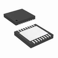
LT3021EDH-1.2#PBF Linear Technology, LT3021EDH-1.2#PBF Datasheet - Page 12

LT3021EDH-1.2#PBF
Manufacturer Part Number
LT3021EDH-1.2#PBF
Description
IC REG LDO 1.2V 500MA 16-DFN
Manufacturer
Linear Technology
Datasheet
1.LT3021ES8PBF.pdf
(16 pages)
Specifications of LT3021EDH-1.2#PBF
Regulator Topology
Positive Fixed
Voltage - Output
1.2V
Voltage - Input
Up to 10V
Voltage - Dropout (typical)
0.155V @ 500mA
Number Of Regulators
1
Current - Output
500mA
Current - Limit (min)
550mA
Operating Temperature
-40°C ~ 125°C
Mounting Type
Surface Mount
Package / Case
16-DFN
Primary Input Voltage
10V
Output Voltage Fixed
1.2V
Dropout Voltage Vdo
155mV
No. Of Pins
16
Output Current
500mA
Operating Temperature Range
-40°C To +125°C
Msl
MSL 1 - Unlimited
Rohs Compliant
Yes
Lead Free Status / RoHS Status
Lead free / RoHS Compliant
Available stocks
Company
Part Number
Manufacturer
Quantity
Price
APPLICATIONS INFORMATION
LT3021/LT3021-1.2/
LT3021-1.5/LT3021-1.8
The LT3021 regulator has internal thermal limiting (with
hysteresis) designed to protect the device during overload
conditions. For normal continuous conditions, do not ex-
ceed the maximum junction temperature rating of 125°C.
Carefully consider all sources of thermal resistance from
junction to ambient including other heat sources mounted
in proximity to the LT3021.
The underside of the LT3021 DH package has exposed
metal (14mm
attached. This allows heat to directly transfer from the
die junction to the printed circuit board metal to control
maximum operating junction temperature. The dual-in-line
pin arrangement allows metal to extend beyond the ends
of the package on the topside (component side) of a PCB.
Connect this metal to GND on the PCB. The multiple IN
and OUT pins of the LT3021 also assist in spreading heat
to the PCB.
The LT3021 S8 package has Pin 4 fused with the lead
frame. This also allows heat to transfer from the die to the
printed circuit board metal, therefore reducing the thermal
resistance. Copper board stiffeners and plated through-
holes can also be used to spread the heat generated by
power devices.
The following tables list thermal resistance for several
different board sizes and copper areas for two different
packages. Measurements were taken in still air on 3/32”
FR-4 board with one ounce copper.
Table 1. Measured Thermal Resistance For DH Package
Table 2. Measured Thermal Resistance For S8 Package
*Device is mounted on topside.
12
TOPSIDE*
TOPSIDE*
2500mm
2500mm
1000mm
900mm
225mm
100mm
225mm
100mm
50mm
50mm
COPPER AREA
COPPER AREA
2
2
2
2
2
2
2
2
2
2
2500mm
2500mm
2500mm
2500mm
2500mm
2500mm
2500mm
2500mm
2500mm
2500mm
BACKSIDE
BACKSIDE
2
) from the lead frame to where the die is
2
2
2
2
2
2
2
2
2
2
BOARD AREA
BOARD AREA
2500mm
2500mm
2500mm
2500mm
2500mm
2500mm
2500mm
2500mm
2500mm
2500mm
2
2
2
2
2
2
2
2
2
2
(JUNCTION-TO-AMBIENT)
(JUNCTION-TO-AMBIENT)
THERMAL RESISTANCE
THERMAL RESISTANCE
30°C/W
35°C/W
50°C/W
55°C/W
65°C/W
70°C/W
70°C/W
78°C/W
84°C/W
96°C/W
Calculating Junction Temperature
Example: Given an output voltage of 1.2V, an input voltage
range of 1.8V ±10%, an output current range of 1mA to
500mA, and a maximum ambient temperature of 70°C,
what will the maximum junction temperature be for an
application using the DH package?
The power dissipated by the device is equal to:
where
so
The thermal resistance is in the range of 35°C/W to 70°C/W
depending on the copper area. So the junction temperature
rise above ambient is approximately equal to:
The maximum junction temperature equals the maximum
junction temperature rise above ambient plus the maximum
ambient temperature or:
Protection Features
The LT3021 incorporates several protection features
that make it ideal for use in battery-powered circuits.
In addition to the normal protection features associated
with monolithic regulators, such as current limiting and
thermal limiting, the device also protects against reverse-
input voltages, reverse-output voltages and reverse out-
put-to-input voltages.
Current limit protection and thermal overload protection
protect the device against current overload conditions at
the output of the device. For normal operation, do not
exceed a junction temperature of 125°C.
The IN pins of the device withstand reverse voltages of
10V. The LT3021 limits current fl ow to less than 1μA and
no negative voltage appears at OUT. The device protects
both itself and the load against batteries that are plugged
in backwards.
I
I
V
I
P = 500mA(1.98V – 1.2V) + 10mA(1.98V) = 0.41W
0.41W(52.5°C/W) = 21.5°C
T
OUT(MAX)
OUT(MAX)
GND
JMAX
IN(MAX)
at (I
= 21.5°C + 70°C = 91.5°C
= 1.98V
OUT
(V
= 500mA
IN(MAX)
= 500mA, V
– V
OUT
IN
) + I
= 1.98V) = 10mA
GND
(V
IN(MAX)
)
3021fc


