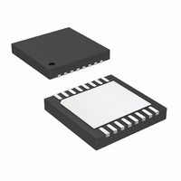
LT3021EDH-1.8#PBF Linear Technology, LT3021EDH-1.8#PBF Datasheet - Page 11

LT3021EDH-1.8#PBF
Manufacturer Part Number
LT3021EDH-1.8#PBF
Description
IC REG LDO 1.8V 500MA 16-DFN
Manufacturer
Linear Technology
Datasheet
1.LT3021ES8PBF.pdf
(16 pages)
Specifications of LT3021EDH-1.8#PBF
Regulator Topology
Positive Fixed
Voltage - Output
1.8V
Voltage - Input
Up to 10V
Voltage - Dropout (typical)
0.155V @ 500mA
Number Of Regulators
1
Current - Output
500mA
Current - Limit (min)
550mA
Operating Temperature
-40°C ~ 125°C
Mounting Type
Surface Mount
Package / Case
16-DFN
Lead Free Status / RoHS Status
Lead free / RoHS Compliant
Available stocks
Company
Part Number
Manufacturer
Quantity
Price
APPLICATIONS INFORMATION
amounts of noise. A ceramic capacitor produced Figure
4’s trace in response to light tapping from a pencil. Similar
vibration induced behavior can masquerade as increased
output voltage noise.
No-Load/Light-Load Recovery
A transient load step occurs when the output current changes
from its maximum level to zero current or a very small load
current. The output voltage responds by overshooting until
the regulator lowers the amount of current it delivers to the
new level. The regulator loop response time and the amount
of output capacitance control the amount of overshoot. Once
the regulator has decreased its output current, the current
provided by the resistor divider (which sets V
only current remaining to discharge the output capacitor
from the level to which it overshot. The amount of time it
takes for the output voltage to recover easily extends to
milliseconds with microamperes of divider current and a
few microfarads of output capacitance.
Figure 3. Ceramic Capacitor Temperature Characteristics
Figure 2. Ceramic Capacitor DC Bias Characteristics
–100
–100
–20
–40
–60
–80
–20
–40
–60
–80
20
40
20
0
0
–50
0
BOTH CAPACITORS ARE 16V,
1210 CASE SIZE, 10μF
–25
2
4
DC BIAS VOLTAGE (V)
0
TEMPERATURE (°C)
BOTH CAPACITORS ARE 16V,
1210 CASE SIZE, 10μF
6
25
8
Y5V
X5R
50
10
Y5V
75
12
X5R
100
14
3021 F02
3021 F03
125
16
OUT
) is the
To eliminate this problem, the LT3021 incorporates a
no-load or light-load recovery circuit. This circuit is a
voltage-controlled current sink that signifi cantly improves
the light load transient response time by discharging the
output capacitor quickly and then turning off. The cur-
rent sink turns on when the output voltage exceeds 6%
of the nominal output voltage. The current sink level is
then proportional to the overdrive above the threshold
up to a maximum of approximately 15mA. Consult the
curve in the Typical Performance Characteristics for the
No-Load Recovery Threshold.
If external circuitry forces the output above the no load
recovery circuit’s threshold, the current sink turns on in
an attempt to restore the output voltage to nominal. The
current sink remains on until the external circuitry releases
the output. However, if the external circuitry pulls the output
voltage above the input voltage, or the input falls below
the output, the LT3021 turns the current sink off and shuts
down the bias current/reference generator circuitry.
Thermal Considerations
The LT3021’s power handling capability is limited by
its maximum rated junction temperature of 125°C. The
power dissipated by the device is comprised of two
components:
1. Output current multiplied by the input-to-output voltage
2. GND pin current multiplied by the input voltage:
GND pin current is found by examining the GND pin current
curves in the Typical Performance Characteristics. Power
dissipation is equal to the sum of the two components
listed above.
Figure 4. Noise Resulting from Tapping on a Ceramic Capacitor
differential: (I
(I
GND
1mV/DIV
)(V
IN
LT3021-1.5/LT3021-1.8
).
V
C
I
LOAD
OUT
OUT
OUT
= 1.3V
= 10F
= 0
LT3021/LT3021-1.2/
)(V
IN
– V
1ms/DIV
OUT
) and
3021 F04
11
3021fc


