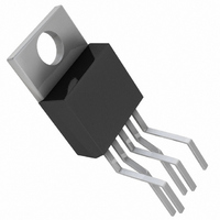
LT1036CT#PBF Linear Technology, LT1036CT#PBF Datasheet - Page 6

LT1036CT#PBF
Manufacturer Part Number
LT1036CT#PBF
Description
IC REG LOGIC CNTRL 12V/5V TO220
Manufacturer
Linear Technology
Datasheet
1.LT1036CTPBF.pdf
(12 pages)
Specifications of LT1036CT#PBF
Regulator Topology
Positive Fixed
Voltage - Output
12V, 5V
Voltage - Input
Up to 30V
Number Of Regulators
2
Current - Output
3A, 75mA
Operating Temperature
0°C ~ 125°C
Mounting Type
Through Hole
Package / Case
TO-220-5 (Bent and Staggered Leads)
Lead Free Status / RoHS Status
Lead free / RoHS Compliant
Voltage - Dropout (typical)
-
Current - Limit (min)
-
Available stocks
Company
Part Number
Manufacturer
Quantity
Price
LT1036
APPLICATIO S I FOR ATIO
The basic shutdown control circuit uses a direct gate drive
or an open collector driver and a pull-up resistor which are
tied to V
Driving the Enable Pin
The enable pin equivalent schematic is shown in Figure 3.
Basically, enable pin current is zero above the threshold
and about 1.5µA below the threshold, flowing out of the
pin. Standard logic, such as TTL and CMOS, will interface
directly to the enable pin, even if the logic output swing is
higher than the input voltage (V
15V CMOS can be used to drive the enable pin, even if
the regulator is not powered up, without loading the
CMOS output.
Timing functions, such as delayed power-up or
power-down can be implemented with an RC network.
The current flowing out of the enable pin should not
6
V
IN
AUX
+
, as shown in Figure 2.
7.5-20V
1µF
1V
5
2
U
IN
EN
V
IN
EN
AUX
LT1036
GND
Figure 3
Figure 1
LT1036
Figure 2
U
GND
3
OUT
AUX
OUT
AUX
70µA
1
4
0mA–75mA
+
W
IN
LOAD
ENABLE
) to the regulator.
2µF
1036 F03
+
5V
2µF
V
5V
O
U
12V
1036 F01
0A-3A
LOAD
1036 F02
12V
be used as the timing current in delayed power-up
applications as it is temperature sensitive and varies
somewhat from device to device. Instead, a resistor tied to
the auxiliary output, the input, or to a logic signal should
be used. The timing resistor chosen should provide at
least 25µA of current to “swamp out” the effects of the
internal current.
Main Output Current Voltage Characteristics
Following a high to low transition at the enable pin, the
main regulator output will begin to drop after a delay of
approximately 0.4µs. With no capacitive load, the output
will fall to zero in approximately 0.8µs (R
With a capacitive load, fall time is limited by the RC product
of the load and the output capacitance. For light loads
(R
internal current pull-down of 15mA for output voltages
down to 1.5V. Below 1.5V, the pull-down current drops to
≈ 4mA. The DC output voltage in the shutdown mode is
approximately 0.12V due to an internal current path in the
regulator. (See Figure 4.)
The user should note that the output in the low state can
only sink about 3mA. If current is forced into the output,
the output voltage will rise to 1V at 5mA and about 1.5V at
10mA. With no output capacitor, the rise time of the main
output is about 12µs. With an output capacitor, rise time
is limited by the short circuit current of the LT1036 and the
load capacitance. A 10µF output capacitor slows the
output rise time to approximately 80µs.
L
>400Ω), the discharge time is controlled by an
10
6
0
9
8
7
5
4
3
2
1
0
T
V
J
IN
= 25°C
0.2
= 15V
T
J
0.4
= 150°C
OUTPUT VOLTAGE (V)
0.6
Figure 4
0.8
1.0
T
J
1.2
= –55°C
1.4
1036 F04
L
= 4Ω to 100Ω).
1.6
1036fb


