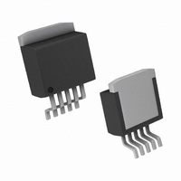
LP3855ESX-5.0/NOPB National Semiconductor, LP3855ESX-5.0/NOPB Datasheet - Page 13

LP3855ESX-5.0/NOPB
Manufacturer Part Number
LP3855ESX-5.0/NOPB
Description
IC REG LDO 1.5A 5.0V TO-263-5
Manufacturer
National Semiconductor
Datasheet
1.LP3852EMP-3.3NOPB.pdf
(20 pages)
Specifications of LP3855ESX-5.0/NOPB
Regulator Topology
Positive Fixed
Voltage - Output
5V
Voltage - Input
Up to 7V
Voltage - Dropout (typical)
0.24V @ 1.5A
Number Of Regulators
1
Current - Output
1.5A (Max)
Operating Temperature
-40°C ~ 125°C
Mounting Type
Surface Mount
Package / Case
TO-263-5, D²Pak (5 leads + Tab), TO-263BA
Lead Free Status / RoHS Status
Lead free / RoHS Compliant
Current - Limit (min)
-
Other names
LP3855ESX-5.0
ground pin current and die size, LP3852/LP3855 achieves
low noise performance and low quiescent current operation.
The total output noise specification for LP3852/LP3855 is
presented in the Electrical Characteristics table. The Output
noise density at different frequencies is represented by a
curve under typical performance characteristics.
SHORT-CIRCUIT PROTECTION
The LP3852 and LP3855 are short circuit protected and in the
event of a peak over-current condition, the short-circuit con-
trol loop will rapidly drive the output PMOS pass element off.
Once the power pass element shuts down, the control loop
will rapidly cycle the output on and off until the average power
dissipation causes the thermal shutdown circuit to respond to
servo the on/off cycling to a lower frequency. Please refer to
the section on thermal information for power dissipation cal-
culations.
ERROR FLAG OPERATION
The LP3852/LP3855 produces a logic low signal at the Er-
ror Flag pin when the output drops out of regulation due to low
SENSE PIN
In applications where the regulator output is not very close to
the load, LP3855 can provide better remote load regulation
using the SENSE pin.
SENSE option. LP3852 regulates the voltage at the output
pin. Hence, the voltage at the remote load will be the regulator
output voltage minus the drop across the trace resistance. For
Figure 4
depicts the advantage of the
FIGURE 3. Error Flag Operation
13
input voltage, current limiting, or thermal limiting. This flag has
a built in hysteresis. The timing diagram in
relationship between the ERROR flag and the output voltage.
In this example, the input voltage is changed to demonstrate
the functionality of the Error Flag.
The internal Error flag comparator has an open drain output
stage. Hence, the ERROR pin should be pulled high through
a pull up resistor. Although the ERROR flag pin can sink cur-
rent of 1mA, this current is energy drain from the input supply.
Hence, the value of the pull up resistor should be in the range
of 10kΩ to 1MΩ. The ERROR pin must be connected to
ground if this function is not used. It should also be noted
that when the shutdown pin is pulled low, the ERROR pin is
forced to be invalid for reasons of saving power in shutdown
mode.
example, in the case of a 3.3V output, if the trace resistance
is 100mΩ, the voltage at the remote load will be 3.15V with
1.5A of load current, I
at the sense pin. Connecting the sense pin to the remote load
will provide regulation at the remote load, as shown in
4. If the sense option pin is not required, the sense pin must
be connected to the V
LOAD
OUT
. The LP3855 regulates the voltage
pin.
20031007
Figure 3
www.national.com
shows the
Figure


