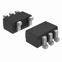
NCP508SQ33T1G ON Semiconductor, NCP508SQ33T1G Datasheet - Page 3

NCP508SQ33T1G
Manufacturer Part Number
NCP508SQ33T1G
Description
IC REG LDO 50MA 3.3V SC-88A
Manufacturer
ON Semiconductor
Datasheet
1.NCP508SQ15T1G.pdf
(15 pages)
Specifications of NCP508SQ33T1G
Regulator Topology
Positive Fixed
Voltage - Output
3.3V
Voltage - Input
Up to 7V
Voltage - Dropout (typical)
0.18V @ 50mA
Number Of Regulators
1
Current - Output
50mA (Min)
Operating Temperature
-40°C ~ 85°C
Mounting Type
Surface Mount
Package / Case
SC-70-5, SC-88A, SOT-353, 16-QFN, SC-70-6, SC-88, SOT-323-6, SOT-363, SOT-23-8
Number Of Outputs
1
Polarity
Positive
Input Voltage Max
13 V
Output Voltage
3.3 V
Output Voltage Tolerance
3 %
Output Type
Fixed
Dropout Voltage (max)
300 mV
Output Current
50 mA
Line Regulation
2 mV
Load Regulation
6 mV
Maximum Operating Temperature
+ 85 C
Mounting Style
SMD/SMT
Minimum Operating Temperature
- 40 C
Lead Free Status / RoHS Status
Lead free / RoHS Compliant
Current - Limit (min)
-
Lead Free Status / Rohs Status
Lead free / RoHS Compliant
Available stocks
Company
Part Number
Manufacturer
Quantity
Price
Company:
Part Number:
NCP508SQ33T1G
Manufacturer:
ON Semiconductor
Quantity:
500
Part Number:
NCP508SQ33T1G
Manufacturer:
ON/安森美
Quantity:
20 000
5. Low duty cycle pulse techniques are used during testing to maintain the junction temperature as close to ambient as possible.
6. Turn on time is defined from Enable at 10% to V
ELECTRICAL CHARACTERISTICS
noted)
Output Voltage Tolerance (T
Output Voltage Tolerance (T
Line Regulation (V
Load Regulation (I
Output Current (V
Dropout Voltage (V
Quiescent Current
Ground Current
Enable Input Threshold Voltage
Enable Input Current (V
Output Turn On Time (Note 6)
Output Short Circuit Current Limit (V
Ripple Rejection (V
Output Noise Voltage (f = 100 Hz to 100 kHz) (V
= 0 V to V
I
I
I
(Enable Input = 0V)
(Enable Input = V
(Enable Input = V
(Enable Input = V
(Enable Input = V
(Voltage Increasing, Output Turns On, Logic High)
(Voltage Decreasing, Output Turns Off, Logic Low)
out
out
out
in
. C
= 30 mA
= 40 mA
= 50 mA
out
out
out
in
out
= 1.0 mF.
in
= V
= V
= V
= 1.0 mA to 50 mA) (Note 5)
= 3.0 V, Measured at V
enable
out
out(nom)
out(nom)
+ 1 V to 12 V, I
in
in
in
in
A
A
, V
, I
, I
, I
= 25°C, I
= −40°C to 85°C, I
= 2.4 V)
out
out
out
in
– 0.1 V)
Characteristic
+ 1 Vdc + 0.5 V
= V
= 1 mA)
= 10 mA)
= 50 mA)
out
out
out
= 0 V)
+ 1 V, I
(V
= 10 mA)
out
in
= 10 mA) (Note 5)
out
= V
out
out
out
– 100 mV)
pp
out
out(nom)
, f = 1 kHz, Io = 10 mA)
= 0 mA)
= 10 mA)
= 1.5 V)
at 95% nominal value. Min and max values T
http://onsemi.com
+ 1.0 V, V
enable
3
= V
in
, C
in
= 1.0 mF, C
Symbol
V
I
I
Reg
Reg
out(nom)
out(max)
V
I
in
enable
I
V
V
th(en)
RR
GND
V
−V
I
out
out
−
Q
n
load
line
out
out
A
= 1.0 mF, T
= −40°C to 85°C, T
Min
100
0.9
−2
−3
50
−
−
−
−
−
−
−
−
−
−
−
−
−
−
−
J
= 25°C, unless otherwise
1100
Typ
140
155
180
145
160
300
250
0.1
8.0
20
70
39
−
−
2
6
−
−
−
jmax
1900
Max
0.15
250
300
200
260
500
+2
+3
20
40
15
= 125°C. V
−
−
1
−
−
−
−
−
mVrms
Unit
mV
mV
mA
mV
mA
mA
mA
mA
dB
ms
%
%
V
enable


