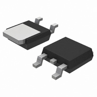
NCP5501DT15G ON Semiconductor, NCP5501DT15G Datasheet - Page 3

NCP5501DT15G
Manufacturer Part Number
NCP5501DT15G
Description
IC REG LINEAR 500MA 1.5V DPAK-4
Manufacturer
ON Semiconductor
Datasheet
1.NCP5501DT50RKG.pdf
(13 pages)
Specifications of NCP5501DT15G
Regulator Topology
Positive Fixed
Voltage - Output
1.5V
Voltage - Input
2.5 ~ 16 V
Number Of Regulators
1
Current - Output
500mA
Current - Limit (min)
500mA
Operating Temperature
-40°C ~ 85°C
Mounting Type
Surface Mount
Package / Case
TO-252-2, DPak (2 Leads + Tab), TO-252AA, SC-63
Number Of Outputs
1
Polarity
Positive
Input Voltage Max
16 V
Output Voltage
1.5 V
Output Type
Fixed
Dropout Voltage (max)
1.073 V at 1 mA
Output Current
500 mA
Line Regulation
0.1 %
Load Regulation
0.35 %
Voltage Regulation Accuracy
2.9 %
Maximum Operating Temperature
+ 85 C
Mounting Style
SMD/SMT
Minimum Operating Temperature
- 40 C
Lead Free Status / RoHS Status
Lead free / RoHS Compliant
Voltage - Dropout (typical)
-
Lead Free Status / Rohs Status
Lead free / RoHS Compliant
Available stocks
Company
Part Number
Manufacturer
Quantity
Price
Part Number:
NCP5501DT15G
Manufacturer:
ON/安森美
Quantity:
20 000
Stresses exceeding Maximum Ratings may damage the device. Maximum Ratings are stress ratings only. Functional operation above the
Recommended Operating Conditions is not implied. Extended exposure to stresses above the Recommended Operating Conditions may affect
device reliability.
*Latchup Current Maximum Rating: ≤ 100 mA per JEDEC standard: JESD78.
1. Refer to Electrical Characteristics and Application Information for Safe Operating Area.
2. Reverse bias protection feature valid only if V
3. Pb−Free, 60 sec –150 sec above 217°C, 40 sec max at peak temperature
4. This device series incorporates ESD protection and is tested by the following methods:
5. Maximum = +16 V or (V
6. As measured using a copper heat spreading area of 650 mm
7. Minimum V
ABSOLUTE MAXIMUM RATINGS
THERMAL CHARACTERISTICS
OPERATING RANGES
Input Voltage (Note 1)
Output, Enable Voltage
Maximum Junction Temperature
Storage Temperature
Moisture Sensitivity Level
Lead Temperature Soldering
Reflow (SMD Styles Only), Pb−Free Versions (Note 3)
ESD Capability, Human Body Model (Note 4)
ESD Capability, Machine Model (Note 4)
ESD Capability, Charged Device Model (Note 4)
Package Dissipation
Thermal Characteristics, DPAK 3 and DPAK 5 (Note 1)
Thermal Resistance, Junction−to−Air (Note 6)
Thermal Resistance, Junction−to−Case
Thermal Characteristics, SOIC−8 (Note 1)
Thermal Resistance, Junction−to−Air (Note 6)
Thermal Reference, Junction−to−Lead
Operating Input Voltage (Note 1)
Adjustable Output Voltage Range (Adjustable Version Only)
Operating Ambient Temperature Range
ESD Human Body Model tested per AEC−Q100−002 (EIA/JESD22−A114)
ESD Machine Model tested per AEC−Q100−003 (EIA/JESD22−A115)
ESD Charged Device Model tested per EIA/JES D22/C101, Field Induced Charge Model
NCP5500, NCP5501
NCV5500, NCV5501
in
= 2.5 V or (V
in
+ 0.3 V), whichever is lower.
out
Rating
Rating
Rating
+ V
DO
), whichever is higher.
out
All Packages
− V
in
v 7 V.
http://onsemi.com
2
, 1 oz copper thickness.
ESD
ESD
3
V
Symbol
Symbol
Symbol
ESD
out
R
MSL
R
R
R
T
V
T
V
P
V
T
T
qJC
YJL
Stg
qJA
qJA
sld
out
, EN
in
in
A
D
J
HBM
CDM
MM
V
out
−0.3 (Note 2)
+ V
(Note 7)
4000
1000
−0.3
1.25
Min
Min
Min
−55
200
−40
−40
−
DO
, 2.5 V
1
Internally Limited
(Notes 2 and 5)
265 Peak
V
+16 or
in
+150
Max
Max
Max
+18
150
125
5.2
5.0
60
80
22
16
85
+ 0.3
−
−
−
°C/W
°C/W
Unit
Unit
Unit
°C
°C
°C
°C
W
V
V
V
V
V
V
V
−


