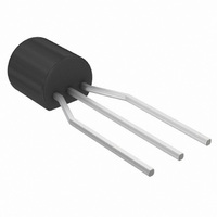
LP2950CZ-3.3RAG ON Semiconductor, LP2950CZ-3.3RAG Datasheet - Page 5

LP2950CZ-3.3RAG
Manufacturer Part Number
LP2950CZ-3.3RAG
Description
IC REG LDO LP 100MA 3.3V TO-92
Manufacturer
ON Semiconductor
Datasheet
1.LP2951ACDR2G.pdf
(23 pages)
Specifications of LP2950CZ-3.3RAG
Regulator Topology
Positive Fixed
Voltage - Output
3.3V
Voltage - Input
Up to 30V
Voltage - Dropout (typical)
0.35V @ 100mA
Number Of Regulators
1
Current - Output
100mA
Operating Temperature
-40°C ~ 125°C
Mounting Type
Through Hole
Package / Case
TO-92-3 (Standard Body), TO-226
Number Of Outputs
1
Polarity
Positive
Input Voltage Max
30 V
Output Voltage
3.3 V
Output Type
Fixed
Dropout Voltage (max)
0.08 V at 100 uA
Output Current
100 mA
Line Regulation
0.2 %
Load Regulation
0.2 %
Voltage Regulation Accuracy
1 %
Maximum Operating Temperature
+ 125 C
Mounting Style
Through Hole
Minimum Operating Temperature
- 40 C
Reference Voltage
1.26 V
Primary Input Voltage
30V
Output Voltage Fixed
3.3V
Dropout Voltage Vdo
350mV
No. Of Pins
3
Operating Temperature Range
-40°C To +125°C
Filter Terminals
Solder
Rohs Compliant
Yes
Lead Free Status / RoHS Status
Lead free / RoHS Compliant
Current - Limit (min)
-
Lead Free Status / Rohs Status
Lead free / RoHS Compliant
Other names
LP2950CZ-3.3RAG
LP2950CZ-3.3RAGOSTR
LP2950CZ-3.3RAGOSTR
Available stocks
Company
Part Number
Manufacturer
Quantity
Price
Company:
Part Number:
LP2950CZ-3.3RAG
Manufacturer:
ON Semiconductor
Quantity:
1 885
Company:
Part Number:
LP2950CZ-3.3RAG
Manufacturer:
ON Semiconductor
Quantity:
1 250
6. The Junction−to−Ambient Thermal Resistance is determined by PCB copper area per Figure 29.
7. ESD data available upon request.
8. Low duty pulse techniques are used during test to maintain junction temperature as close to ambient as possible.
9. V
10. Noise tests on the LP2951 are made with a 0.01 mF capacitor connected across Pins 7 and 1.
*NCV prefix is for automotive and other applications requiring site and change control.
ELECTRICAL CHARACTERISTICS (continued)
unless otherwise noted.)
LP2951A/LP2951AC Only
Error Comparator
Shutdown Input
Line Regulation (V
Load Regulation (I
Dropout Voltage
Supply Bias Current
Dropout Supply Bias Current (V
Current Limit (V
Thermal Regulation
Output Noise Voltage (10 Hz to 100 kHz) (Note 10)
Reference Voltage (T
Reference Voltage (T
Reference Voltage (T
Feedback Pin Bias Current
Output Leakage Current (V
Output Low Voltage (V
Upper Threshold Voltage (V
Lower Threshold Voltage (V
Hysteresis (V
Input Logic Voltage
Shutdown Pin Input Current
Regulator Output Current in Shutdown Mode
I
LP2950C−XX/LP2951C/LP2951C−XX/NCV2951C*
LP2950AC−XX/LP2951AC/LP2951AC−XX/NCV2951AC*
LP2950C−XX/LP2951C/LP2951C−XX/NCV2951C*
LP2950AC−XX/LP2951AC/LP2951AC−XX/NCV2951AC*
I
I
I
I
C
C
LP2951C/LP2951C−XX/NCV2951C*
LP2951AC/LP2951AC−XX/NCV2951AC*
LP2951C/LP2951C−XX/NCV2951C*
LP2951AC/LP2951AC−XX/NCV2951AC*
I
Logic “0” (Regulator “On”)
Logic “1” (Regulator “Off”)
V
V
(V
O
O(nom)
O
O
O
O
O
shtdn
shtdn
L
L
= 100 mA) (Note 9)
LP2951C/LP2951C−XX/NCV2951C*
LP2951AC/LP2951AC−XX/NCV2951AC*
in
= 100 mA
= 100 mA
= 100 mA
= 100 mA
= 100 mA to 100 mA, V
= 1.0 mF
= 100 mF
= 30 V, V
= 2.4 V
= 30 V
is the part number voltage option.
in
= 6.0 V)
shtdn
O
Shorted to Ground)
O
in
= 100 mA to 100 mA)
= V
= 2.0 V, V
A
A
A
in
= 25°C)
= − 40 to +125°C)
= − 40 to +125°C)
O(nom)
= 4.5 V, I
Characteristic
OH
in
in
in
= 23 to 30 V
= 6.0 V)
= 6.0 V)
= 30 V)
O
+1.0 V to 30 V) (Note 9)
in
= 0, Pin 6 Connected to Pin 7)
= V
OL
= 400 mA)
O(nom)
− 0.5 V,
(V
in
http://onsemi.com
= V
O
+ 1.0 V, I
5
Reg
I
Symbol
CCdropout
Reg
V
Reg
V
O
I
I
I
V
V
shtdn
V
V
V
V
V
I
Limit
I
I
shtdn
V
I
− V
CC
thermal
FB
lkg
= 100 mA, C
off
thu
ref
ref
ref
OL
thl
hy
load
n
line
O
O
1.210
1.220
1.200
1.200
1.185
1.190
Min
2.0
40
= 1.0 mF, T
−
−
−
−
−
−
−
−
−
−
−
−
−
−
−
−
−
−
0
−
−
−
A
= 25°C [Note 8],
1.235
1.235
0.08
0.04
0.13
0.05
0.05
0.01
Typ
350
110
220
126
150
450
4.0
3.0
30
93
56
15
45
60
15
35
−
−
−
−
−
−
1.260
1.250
1.270
1.260
1.285
1.270
Max
0.20
0.10
0.20
0.10
0.20
450
120
170
300
250
600
1.0
0.7
80
12
40
95
30
50
10
−
−
−
−
mVrms
%/W
Unit
mV
mA
mA
mV
mV
mV
mV
mA
mA
nA
mA
mA
mA
%
%
V
V
V
V


