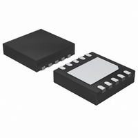
NCP3335AMN150R2G ON Semiconductor, NCP3335AMN150R2G Datasheet - Page 13

NCP3335AMN150R2G
Manufacturer Part Number
NCP3335AMN150R2G
Description
IC REG LDO 500MA 1.5V 10-DFN
Manufacturer
ON Semiconductor
Datasheet
1.NCP3335ADM150R2G.pdf
(21 pages)
Specifications of NCP3335AMN150R2G
Regulator Topology
Positive Fixed
Voltage - Output
1.5V
Voltage - Input
2.6 ~ 12 V
Voltage - Dropout (typical)
0.94V @ 500mA
Number Of Regulators
1
Current - Output
500mA (Min)
Operating Temperature
-40°C ~ 85°C
Mounting Type
Surface Mount
Package / Case
10-VFDFN Exposed Pad
Number Of Outputs
1
Polarity
Positive
Input Voltage Max
16 V
Output Voltage
1.5 V
Output Type
Fixed
Dropout Voltage (max)
1.43 V at 500 mA
Output Current
0.86 A
Line Regulation
0.04 mV / V
Load Regulation
0.04 mV / mA
Voltage Regulation Accuracy
0.9 %
Maximum Operating Temperature
+ 150 C
Mounting Style
SMD/SMT
Minimum Operating Temperature
- 40 C
Lead Free Status / RoHS Status
Lead free / RoHS Compliant
Current - Limit (min)
-
Lead Free Status / Rohs Status
Lead free / RoHS Compliant
Other names
NCP3335AMN150R2G
NCP3335AMN150R2GOSTR
NCP3335AMN150R2GOSTR
Available stocks
Company
Part Number
Manufacturer
Quantity
Price
Company:
Part Number:
NCP3335AMN150R2G
Manufacturer:
ON Semiconductor
Quantity:
2 350
Part Number:
NCP3335AMN150R2G
Manufacturer:
ON/安森美
Quantity:
20 000
25. Performance guaranteed over the operating temperature range by design and/or characterization, production tested at T
26. For output current capability for T
27. T
28. Reverse bias protection feature valid only if V
ELECTRICAL CHARACTERISTICS – Adjustable
Note 25)
Reference Voltage (Accuracy)
Reference Voltage (Accuracy)
Reference Voltage (Accuracy) (Note 26)
Line Regulation
Load Regulation
Dropout Voltage (See App Note), V
Peak Output Current (Note 27) (See Figure 16)
Short Output Current (See Figure 16)
Thermal Shutdown
Ground Current
Output Noise
Shutdown
S
Output Current In Shutdown Mode, V
Reverse Bias Protection, Current Flowing from the Output Pin to GND
D
duty cycle pulse techniques are used during testing to maintain the junction temperature as close to ambient as possible.
A
V
V
V
V
V
I
I
I
I
In Regulation
In Dropout
In Shutdown
C
C
Threshold Voltage ON
Threshold Voltage OFF
Input Current, V
(V
load
load
load
load
in
in
in
in
in
nr
nr
must be greater than 0°C.
in
I
I
I
I
V
S
= 2.9 V to V
= 2.9 V to V
= 2.9 V to V
= 2.9 V to 12 V, I
= 2.9 V, I
= 0 nF, I
= 10 nF, I
load
load
load
load
= 0 V, V
= 500 mA (Note 27)
= 300 mA
= 50 mA
= 0.1 mA
in
D
= V
= 0 V
= 500 mA (Note 27)
= 300 mA (Note 27)
= 50 mA
= 0.1 mA
out
load
out_forced
load
load
-0.1 V or 2.2 V (whichever is higher), I
out
out
out
SD
= 500 mA, f = 10 Hz to 100 kHz, C
= 0.1 mA to 500 mA
= 500 mA, f = 10 Hz to 100 kHz, C
+ 4.0 V, I
+ 4.0 V, I
+ 4.0 V, I
= 0 V to 0.4 V or V
load
= V
= 0.1 mA
out
load
load
load
(nom) ≤ 7 V) (Note 28)
Characteristic
= 0.1 mA to 500 mA, T
= 0.1 mA to 500 mA, T
= 0.1 mA to 500 mA, T
out
A
out
< 0°C, please refer to Figures 18 to 22.
= 2.5 V to 10 V
= 0 V
SD
= 2.0 V to V
out
- V
out
in
load
out
≤ 7 V.
(V
in
http://onsemi.com
= 10 mF
A
A
A
out
= 10 mF
= 25°C
= 0°C to +85°C
= 0.1 mA
= -40°C to +125°C
NCP3335A
= 1.25 V typical, V
13
V
V
V
V
out
out
in
in
> 3.3 V
> 5.4 V
≤ 3.3 V
≤ 5.4 V
in
= 2.9 V, T
Load
Symbol
Line
I
V
I
GNDsh
I
I
OUTR
V
V
V
V
GND
OSD
Ipk
I
noise
I
T
SD
DO
sc
ref
ref
ref
J
Reg
Reg
A
= -40°C to +85°C, unless otherwise noted,
-0.9%
-1.4%
-1.5%
1.239
1.233
1.231
Min
500
2.0
1.25
1.25
1.25
0.04
0.04
0.07
0.07
0.07
Typ
700
160
9.0
4.6
0.8
1.0
38
26
-
-
+0.9%
+1.4%
+1.5%
1.261
1.268
1.269
J
Max
340
230
110
860
900
990
190
500
7.5
2.5
1.0
0.4
1.0
5.0
1.0
10
14
= T
A
= 25°C. Low
mV/mA
mVrms
mVrms
mV/V
Unit
mV
mA
mA
mA
°C
mA
mA
mA
mA
mA
mA
V
V
V
V
V


