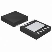
NCV8535MN150R2G ON Semiconductor, NCV8535MN150R2G Datasheet - Page 13

NCV8535MN150R2G
Manufacturer Part Number
NCV8535MN150R2G
Description
IC REG LDO 500MA 1.5V 10-DFN
Manufacturer
ON Semiconductor
Datasheet
1.NCV8535MN150R2G.pdf
(22 pages)
Specifications of NCV8535MN150R2G
Regulator Topology
Positive Fixed
Voltage - Output
1.5V
Voltage - Input
2.9 ~ 12 V
Voltage - Dropout (typical)
0.94V @ 500mA
Number Of Regulators
1
Current - Output
500mA
Operating Temperature
-40°C ~ 85°C
Mounting Type
Surface Mount
Package / Case
10-VFDFN Exposed Pad
Number Of Outputs
1
Polarity
Positive
Input Voltage Max
12 V
Output Voltage
1.5 V
Output Type
Fixed
Dropout Voltage (max)
1.43 V at 500 mA
Output Current
860 mA
Line Regulation
0.04 mV / V
Load Regulation
0.04 mV / mA
Voltage Regulation Accuracy
0.9 %
Maximum Operating Temperature
+ 150 C
Mounting Style
SMD/SMT
Minimum Operating Temperature
- 40 C
Reference Voltage
1.261 V
Lead Free Status / RoHS Status
Lead free / RoHS Compliant
Current - Limit (min)
-
Lead Free Status / Rohs Status
Lead free / RoHS Compliant
Available stocks
Company
Part Number
Manufacturer
Quantity
Price
Company:
Part Number:
NCV8535MN150R2G
Manufacturer:
ON Semiconductor
Quantity:
500
Part Number:
NCV8535MN150R2G
Manufacturer:
ON/安森美
Quantity:
20 000
23. Performance guaranteed over the operating temperature range by design and/or characterization, production tested at T
24. For output current capability for T
25. T
26. Maximum dropout voltage is limited by minimum input voltage V
ELECTRICAL CHARACTERISTICS − 1.8 V
Output Voltage (Accuracy)
Output Voltage (Accuracy)
Output Voltage (Accuracy), (Note 24)
Line Regulation
Load Regulation
Dropout Voltage (See App Note)
Peak Output Current (See Figure 16)
Short Output Current (See Figure 16)
Thermal Shutdown
Ground Current
Output Noise
Shutdown
S
Output Current In Shutdown Mode, V
Reverse Bias Protection, Current Flowing from the Output Pin to GND
D
duty cycle pulse techniques are used during testing to maintain the junction temperature as close to ambient as possible.
A
V
V
V
V
V
I
I
I
In Regulation
In Dropout
In Shutdown
C
C
Threshold Voltage ON
Threshold Voltage OFF
(V
Input Current, V
load
load
load
in
in
in
in
in
nr
nr
must be greater than 0°C.
in
I
I
I
I
V
S
= 2.9 V to 5.8 V, I
= 2.9 V to 5.8 V, I
= 2.9 V to 5.8 V, I
= 2.9 V to 12 V, I
= 2.9 V, I
= 0 nF, I
= 10 nF, I
load
load
load
load
= 0 V, V
= 500 mA (Notes 25, 26)
= 300 mA (Notes 25, 26)
= 50 mA (Notes 25, 26)
in
D
= 2.2 V, I
= 0 V
= 50 mA
= 0.1 mA
= 500 mA (Note 25)
= 300 mA (Note 25)
load
out_forced
load
load
load
SD
= 500 mA, f = 10 Hz to 100 kHz, C
= 0.1 mA to 500 mA
= 500 mA, f = 10 Hz to 100 kHz, C
= 0 V to 0.4 V or V
= 0.1 mA
load
load
load
load
= 1.8 V)
= 0.1 mA
= 0.1 mA to 500 mA, T
= 0.1 mA to 500 mA, T
= 0.1 mA to 500 mA, T
Characteristic
A
out
< 0°C, please refer to Figure 21.
= 0 V
SD
= 2.0 V to V
(V
A
A
A
out
= −40°C to +125°C
= 25°C
= 0°C to +85°C
out
= 1.8 V typical, V
out
in
= 10 mF
http://onsemi.com
= 10 mF
in
13
= 2.9 V recommended for guaranteed operation.
in
= 2.9 V, T
A
Load
Symbol
Line
= −40°C to +85°C, unless otherwise noted, Note 23.)
I
V
I
GNDsh
I
I
OUTR
V
V
V
V
GND
OSD
I
noise
I
I
T
SD
pk
out
out
out
DO
sc
J
Reg
Reg
−0.9%
−1.4%
−1.5%
1.783
1.774
1.773
Min
500
2.0
0.04
0.04
0.07
0.07
0.07
Typ
620
230
700
160
1.8
1.8
1.8
9.0
4.6
0.8
95
52
33
10
−
+0.9%
+1.4%
+1.5%
1.817
1.826
1.827
1130
1130
1130
Max
J
830
900
190
500
7.5
2.5
1.0
0.4
1.0
1.0
14
= T
A
= 25°C. Low
mV/mA
mVrms
mVrms
mV/V
Unit
mV
mA
mA
mA
°C
mA
mA
mA
mA
mA
mA
V
V
V
V
V


