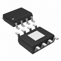
MAX15006AASA+T Maxim Integrated Products, MAX15006AASA+T Datasheet - Page 10

MAX15006AASA+T
Manufacturer Part Number
MAX15006AASA+T
Description
IC REG LINEAR 3.3V 8-SOIC
Manufacturer
Maxim Integrated Products
Datasheet
1.MAX15006CATTT.pdf
(14 pages)
Specifications of MAX15006AASA+T
Regulator Topology
Positive Fixed
Voltage - Output
3.3V
Voltage - Input
4 ~ 40 V
Number Of Regulators
1
Current - Output
50mA (Min)
Current - Limit (min)
80mA
Operating Temperature
-40°C ~ 125°C
Mounting Type
Surface Mount
Package / Case
8-SOIC (3.9mm Width) Exposed Pad, 8-eSOIC. 8-HSOIC
Number Of Outputs
1
Polarity
Positive
Input Voltage Max
40 V
Output Voltage
3.3 V
Output Type
Fixed
Dropout Voltage (max)
0.7 V at 50 mA
Output Current
0.05 A
Line Regulation
0.25 %
Load Regulation
0.7 %
Maximum Power Dissipation
1860 mW
Maximum Operating Temperature
+ 125 C
Mounting Style
SMD/SMT
Minimum Operating Temperature
- 40 C
Lead Free Status / RoHS Status
Lead free / RoHS Compliant
Voltage - Dropout (typical)
-
Lead Free Status / Rohs Status
Lead free / RoHS Compliant
40V, Ultra-Low Quiescent-Current
Linear Regulators in 6-Pin TDFN/8-Pin SO
The MAX15006C/MAX15007C provide an adjustable
output voltage from 1.8V to 10V and do not operate in a
preset output voltage mode. Connect an external resis-
tive divider from OUT to FB to GND as shown in Figure
4 to set the desired output voltage. V
as follows:
where V
required in the external divider for stability.
The MAX15006/MAX15007 provide up to 50mA of contin-
uous output current. The input voltage range extends to
40V. Package power dissipation limits the amount of out-
put current available for a given input/output voltage and
ambient temperature. Figure 5 shows the maximum
allowable power dissipation for these devices to keep the
junction temperature below +150°C. Figure 5 assumes
that the exposed metal pad of the MAX15006/MAX15007
is soldered to 1in
Use Figure 5 to determine the allowable package dissi-
pation for a given ambient temperature. Alternately, use
the following formulas to calculate the allowable pack-
age dissipation. For the TDFN package:
Figure 4. Setting the Adjustable Output Voltage
10
P
D
OFF
=
+4V TO +40V
⎧
⎪
⎨
⎪
⎩ ⎩
______________________________________________________________________________________
ON
0.1μF
1 9048
1 9048
.
.
Available Output Current Calculation
FB
W for T
W
= 1.23V and a 5μA minimum current is
−
0 0238
.
Applications Information
V
2
A
OUT
≤ +
IN
EN
of PCB copper.
°
W W
70
C
MAX15007C
=
°
x T
C
(
GND
V
FB
Output Voltage Setting
A
– 70
×
⎛
⎝ ⎜
°
C for
1
OUT
FB
)
+
R2
R1
+
V
V
OUT
FB
70
OUT
⎞
⎠ ⎟
= 1.23V
° <
= V
C T
R1
R2
FB
is calculated
(1 + R1/R2)
+1.8V TO +10V
A
≤ +
125
2.2μF
°
C
⎫
⎪
⎬
⎪
⎭
For the SO-EP package:
After determining the allowable package dissipation,
calculate the maximum allowable output current, with-
out exceeding the +150°C junction temperature, using
the following formula:
The above equations do not include the negligible
power dissipation from self-heating due to the IC
ground current.
Example 1 (TDFN Package):
T
V
V
Calculate the maximum allowable package dissipation
at the given temperature as follows:
And establish the maximum output current:
Figure 5. Calculated Maximum Power Dissipation vs. Ambient
Temperature
P
P
A
IN
OUT
D
D
=
= +125°C
=
= 26V
⎧
⎪
⎨
⎪
⎩ ⎩
1.9048W
1 8605
1 8605
= 3.3V
.
.
I
OUT(MAX)
I
W for T
W
OUT(MAX)
2.4
2.2
2.0
1.8
1.6
1.4
1.2
1.0
0.8
0.6
0.4
0.2
−
0
0 0233
−
0
.
A
0.0238
1.9408W
(6-PIN TDFN)
1.8605W
(8-PIN SO-EP)
≤ +
20
°
W W
70
=
C
=
°
x T
26V 3.3V
40
C
595.8mW
V
(
°
W
TEMPERATURE (°C)
IN
C
A
60
(
– 70
−
−
125 C
DERATE
23.3mW/°C
P
D
V
°
OUT
80
C for
°
)
100
=
−
DERATE
23.8mW/°C
≤
+
26.2mA
70 C
70
50mA
120
°
° <
C T
)
=
140
A
5
≤ +
9 9 5.8mW
125
°
C
⎫
⎪
⎬
⎪
⎭


