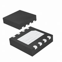
MAX1935ETA15+T Maxim Integrated Products, MAX1935ETA15+T Datasheet - Page 9

MAX1935ETA15+T
Manufacturer Part Number
MAX1935ETA15+T
Description
IC REG LINEAR 500MA 8-TDFN
Manufacturer
Maxim Integrated Products
Datasheet
1.MAX1935ETAT.pdf
(10 pages)
Specifications of MAX1935ETA15+T
Regulator Topology
Positive Fixed
Voltage - Output
1.5V
Voltage - Input
2.25 ~ 5.5 V
Number Of Regulators
1
Current - Output
500mA (Min)
Operating Temperature
-40°C ~ 85°C
Mounting Type
Surface Mount
Package / Case
8-TDFN Exposed Pad
Number Of Outputs
1
Polarity
Positive
Input Voltage Max
5.5 V
Output Voltage
1.5 V
Output Type
Fixed
Output Current
500 mA
Line Regulation
0 % / V
Voltage Regulation Accuracy
2.5 %
Maximum Power Dissipation
1.95 W
Maximum Operating Temperature
+ 85 C
Mounting Style
SMD/SMT
Minimum Operating Temperature
- 40 C
Reference Voltage
0.8 V
Lead Free Status / RoHS Status
Lead free / RoHS Compliant
Voltage - Dropout (typical)
-
Current - Limit (min)
-
Lead Free Status / Rohs Status
Lead free / RoHS Compliant
response graphs (see the Typical Operating
Characteristics) show two components of the output
response: a DC shift from the output impedance due to
the load current change, and the transient response. A
typical transient overshoot for a step change in the load
current from 5mA to 500mA is 40mV. Increasing the
output capacitor’s value and decreasing the ESR
attenuates the overshoot.
A regulator’s minimum input-to-output voltage differential
(dropout voltage) determines the lowest usable supply
voltage. In battery-powered systems, this determines the
useful end-of-life battery voltage. Because the MAX1806
uses a P-channel MOSFET pass transistor, its dropout
voltage is a function of drain-to-source on-resistance
(R
Operating Characteristics):
TRANSISTOR COUNT: 949
Figure 2. Adjustable Output Using External Feedback Resistors
DS(ON)
+2.25V TO +5.5V
ON
OFF
V
V
DROPOUT
IN
) multiplied by the load current (see the Typical
1µF
C
IN
Input-Output (Dropout) Voltage
IN
IN
SHDN
POK
= V
_______________________________________________________________________________________
IN
MAX1935
- V
500mA, Low-Voltage Linear Regulator
OUT
Chip Information
GND
OUT
OUT
SET
= R
DS(ON)
C
10µF
OUT
R1 = R2
✕
I
OUT
V
R
R
0.8V
OUT
2
1
V
- 1
OUT
Figure 3. Power Operating Regions: Maximum Output Current
vs. Input-Output Voltage Difference
600
500
400
300
200
100
0
0
0.5
INPUT-OUTPUT VOLTAGE DIFFERENCE (V)
1.0
1.5
2.0
T
A
in Tiny QFN
= +85°C
2.5
T
A
3.0
= +70°C
3.5
4.0
4.5
5.0
9


