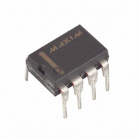
MAX883EPA+ Maxim Integrated Products, MAX883EPA+ Datasheet - Page 9

MAX883EPA+
Manufacturer Part Number
MAX883EPA+
Description
IC REG LINEAR 5V/ADJ 200MA 8-DIP
Manufacturer
Maxim Integrated Products
Datasheet
1.MAX882CSA.pdf
(17 pages)
Specifications of MAX883EPA+
Regulator Topology
Positive Fixed or Adjustable
Voltage - Output
5V, 1.25 ~ 11 V
Voltage - Input
2.9 ~ 11.5 V
Voltage - Dropout (typical)
0.22V @ 200mA
Number Of Regulators
1
Current - Output
200mA
Operating Temperature
0°C ~ 70°C
Mounting Type
Through Hole
Package / Case
8-DIP (0.300", 7.62mm)
Number Of Outputs
1
Polarity
Positive
Input Voltage Max
11.5 V
Output Voltage
1.25 V to 11 V, 5 V
Output Type
Adjustable, Fixed
Dropout Voltage (max)
0.22 V at 100 mA
Output Current
200 mA
Line Regulation
40 mV
Load Regulation
100 mV
Voltage Regulation Accuracy
5 %
Maximum Power Dissipation
0.727 W
Maximum Operating Temperature
+ 85 C
Mounting Style
Through Hole
Minimum Operating Temperature
- 40 C
Reference Voltage
1.24 V
Lead Free Status / RoHS Status
Lead free / RoHS Compliant
Current - Limit (min)
-
Lead Free Status / Rohs Status
Lead free / RoHS Compliant
The MAX882/MAX883/MAX884 also include a foldback
current limiter. It monitors and controls the pass transis-
tor’s gate voltage, estimating the output current and
limiting it to 430mA for output voltages above 0.8V and
(V
0.8V, implying a short-circuit condition, the output cur-
rent is limited to 170mA. The output can be shorted to
ground for 1min without damaging the device if the
package can dissipate (V
ing T
and (V
limiting is allowed, to provide maximum load drive.
Thermal overload protection limits total power dissipa-
tion in the MAX882/MAX883/MAX884. When the junc-
tion temperature exceeds T
sensor sends a signal to the shutdown logic, turning off
the pass transistor and allowing the IC to cool. The
thermal sensor turns the pass transistor on again after
the IC’s junction temperature cools by 10°C, resulting in
a pulsed output during thermal overload conditions.
Thermal overload protection is designed to protect the
MAX882/MAX883/MAX884 if fault conditions occur. It is
not intended to be used as an operating mode.
Prolonged operation in thermal-shutdown mode may
reduce the IC’s reliability. For continual operation, do
not exceed the absolute maximum junction temperature
rating of T
Figure 2. Adjustable Output Using External Feedback
Resistors
IN
INPUT
VOLTAGE
V
O.1µF
OUT
( ) ARE FOR MAX882.
- V
J
C
IN
IN
= +150°C. When the output is greater than 0.8V
= V
OUT
SET
- V
J
R1 + R2
= +150°C.
) > 0.7V. If the output voltage drops below
OUT
R2
OFF
(STBY)
IN
LBI
, V
) < 0.7V (dropout operation), no current
SET
Thermal Overload Protection
_______________________________________________________________________________________
MAX882
MAX883
MAX884
= 1.20V
Foldback Current Limiting
GND
IN
5V/3.3V or Adjustable, Low-Dropout,
x 170mA) without exceed-
J
OUT
SET
= +160°C, the thermal
Low I
R1
R2
C
2.2µF
OUT
VOLTAGE
OUTPUT
Q
LOAD
, 200mA Linear Regulators
Maximum power dissipation of the MAX882/MAX883/
MAX884 depends on the thermal resistance of the case
and PC board, the temperature difference between the
die junction and ambient air, and the rate of
air flow. The power dissipation across the device is
P = I
is as follows:
where (T
the MAX882/MAX883/MAX884 die junction and the sur-
rounding air, θ
the package chosen, and θ
through the PC board, copper traces, and other materi-
als to the surrounding air.
The 8-pin small-outline package for the MAX882/
MAX883/MAX884 features a special lead frame with a
lower thermal resistance and higher allowable power
dissipation. This package’s thermal resistance package
is θ
8-pin plastic DIP package and θ
pin ceramic DIP package.
Figure 3. Setting an Undervoltage Lockout Threshold Using
STBY
INPUT
VOLTAGE
Power Dissipation and Operating Region
JB
V
O.1µF
OUT
STBY TRIP
C
= 53°C/W, compared with θ
IN
J
(V
- T
= V
IN
R1
R2
STBY
A
- V
) is the temperature difference between
JB
R1+ R2
OUT
R2
(or θ
P
IN
LBI
STBY
=
, V
). The resulting power dissipation
STBY
(
JC
θ
(T
JB
MAX882
) is the thermal resistance of
= 1.20V
J
GND
BA
−
+
θ
T )
A
is the thermal resistance
BA
JB
SET
)
JB
OUT
= 125°C/W for an 8-
= 110°C/W for an
C
2.2µF
OUT
VOLTAGE
OUTPUT
9


