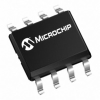
TC1300R-3.3VUA Microchip Technology, TC1300R-3.3VUA Datasheet - Page 8

TC1300R-3.3VUA
Manufacturer Part Number
TC1300R-3.3VUA
Description
IC REG LDO 3.3V 300MA SD 8MSOP
Manufacturer
Microchip Technology
Datasheet
1.TC1300R-2.5VUA.pdf
(16 pages)
Specifications of TC1300R-3.3VUA
Regulator Topology
Positive Fixed
Voltage - Output
3.3V
Voltage - Input
Up to 6V
Voltage - Dropout (typical)
0.21V @ 300mA
Number Of Regulators
1
Current - Output
300mA (Min)
Operating Temperature
-40°C ~ 125°C
Mounting Type
Surface Mount
Package / Case
8-MSOP, Micro8™, 8-uMAX, 8-uSOP,
Primary Input Voltage
6V
Output Voltage Fixed
3.3V
Dropout Voltage Vdo
210mV
No. Of Pins
8
Output Current
300mA
Operating Temperature Range
-40°C To +125°C
Termination Type
SMD
Number Of Outputs
1
Polarity
Positive
Input Voltage Max
6 V
Output Voltage
3.3 V
Output Type
Fixed
Dropout Voltage (max)
0.03 V at 100 uA
Line Regulation
0.02 %
Load Regulation
0.5 %
Voltage Regulation Accuracy
0.5 %
Maximum Operating Temperature
+ 125 C
Mounting Style
SMD/SMT
Minimum Operating Temperature
- 40 C
Lead Free Status / RoHS Status
Lead free / RoHS Compliant
Current - Limit (min)
-
Lead Free Status / Rohs Status
Lead free / RoHS Compliant
Other names
TC1300R3.3VUA
Available stocks
Company
Part Number
Manufacturer
Quantity
Price
Part Number:
TC1300R-3.3VUA
Manufacturer:
MICROCHIP/微芯
Quantity:
20 000
TC1300
3.0
The TC1300 is a combination of a fixed output, low
dropout
monitor/RESET. Unlike bipolar regulators, the TC1300
supply current does not increase with load current. In
addition, V
over the entire specified operating load range (0 mA to
300 mA) and operating input voltage range (2.7V to
6.0V).
Figure 3-1 shows a typical application circuit. The reg-
ulator is enabled any time the shutdown input (SHDN)
is above V
when SHDN is at or below V
trolled by a CMOS logic gate or an I/O port of a micro-
controller. If the SHDN input is not required, it should be
connected directly to the input supply. While in shut-
down, supply current decreases to 30 µA (typical),
V
3.1
The RESET output is driven active-low within 160 µsec
of V
RESET is maintained active for a minimum of
140 msec after V
The TC1300 has an active-low RESET output. The out-
put of the TC1300 is valid down to V
optimized to reject fast transient glitches on the V
line.
FIGURE 3-1:
3.2
A 1 µF (min) capacitor from V
A 1 µF capacitor should also be connected from V
GND if there is more than 10 inches of wire between
the regulator and the AC filter capacitor, or if a battery
is used as the power source. As with all low dropout
regulators, a minimum output capacitance is required
to stabilize the output voltage. For the TC1300, a mini-
mum of 1 µF of output capacitance is enough to stabi-
lize the device over the entire operating load and line
range. The selected output capacitor plays an impor-
tant role is compensating the LDO regulator. For the
DS21385C-page 8
OUT
V
OUT
Microcontroller
DET
falls to zero and RESET remains valid.
RESET
DETAILED DESCRIPTION
RESET Output
Output Capacitor
falling through the reset voltage threshold.
OUT
C
1 µF
IH
regulator
C
470 pF
(Optional)
1
. The regulator is shutdown (disabled)
BYPASS
remains stable and within regulation
DET
1
2
3
4
Bypass
GND
V
rises above the reset threshold.
RESET
Typical Application Circuit.
OUT
TC1300
and
OUT
SHDN
IL
V
Shutdown Control
(from Power
Control Logic)
. SHDN may be con-
DET
V
NC
to ground is required.
IN
a
8
7
6
5
DET
C
1 µF
microcontroller
2
= 1V and is
Battery
V
DET
IN
DET
to
TC1300, the selected output capacitor equivalent
series resistance (ESR) range is 0.1 ohms to 5 ohms
when using 1 µF of output capacitance, and 0.01 ohms
to 5 ohms when using 10 µF of output capacitance.
Because of the ESR requirement, tantalum and alumi-
num electrolytic capacitors are recommended. Alumi-
num electrolytic capacitors are not recommended for
operation at temperatures below -25°C. When operat-
ing from sources other than batteries, rejection and
transient responses can be improved by increasing the
value of the input and output capacitors and employing
passive filtering techniques.
3.3
An optional 470 pF capacitor connected from the
Bypass input to ground reduces noise present on the
internal reference, which in turn significantly reduces
output noise and improves PSRR performance. This
input may be left unconnected. Larger capacitor values
may be used, but results in a longer time period to rated
output voltage when power is initially applied.
3.4
The turn-on response is defined as two separate
response categories, Wake-Up Time (t
Time (t
The TC1300 has a fast Wake-Up Time (10 µsec typi-
cal) when released from shutdown. See Figure 3-2 for
the Wake-Up Time designated as t
Time is defined as the time it takes for the output to rise
to 2% of the V
shutdown.
The total turn-on response is defined as the Settling
Time (t
t
within 2% of its fully enabled value (50 µsec typical)
when released from shutdown. The settling time of the
output voltage is dependent on load conditions and
output capacitance on V
FIGURE 3-2:
WK
SHDN
V
OUT
) is defined as the condition when the output is
S
S
).
) (see Figure 3-2). Settling Time (inclusive with
Bypass Input (Optional)
Turn On Response
V
OUT
IL
value after being released from
Wake-Up Response Time.
OUT
2002 Microchip Technology Inc.
(RC response).
WK
2%
WK
. The Wake-Up
t
V
WK
98%
IH
) and Settling
t
S


