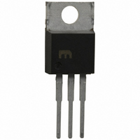
MIC29300-3.3BT Micrel Inc, MIC29300-3.3BT Datasheet - Page 17

MIC29300-3.3BT
Manufacturer Part Number
MIC29300-3.3BT
Description
IC REG LDO 3A 3.3V TO220-3
Manufacturer
Micrel Inc
Datasheet
1.MIC29152WU_TR.pdf
(23 pages)
Specifications of MIC29300-3.3BT
Regulator Topology
Positive Fixed
Voltage - Output
3.3V
Voltage - Input
Up to 26V
Voltage - Dropout (typical)
0.37V @ 3A
Number Of Regulators
1
Current - Output
3A
Operating Temperature
-40°C ~ 125°C
Mounting Type
Through Hole
Package / Case
TO-220-3 (Straight Leads)
Primary Input Voltage
26V
Output Voltage Fixed
3.3V
Dropout Voltage Vdo
350mV
No. Of Pins
3
Output Current
3A
Operating Temperature Range
-40°C To +125°C
Termination Type
Through Hole
Lead Free Status / RoHS Status
Lead free / RoHS Compliant
Current - Limit (min)
-
Lead Free Status / RoHS Status
Contains lead / RoHS non-compliant, Lead free / RoHS Compliant
Available stocks
Company
Part Number
Manufacturer
Quantity
Price
Part Number:
MIC29300-3.3BT
Manufacturer:
MIC
Quantity:
20 000
Application Information
The
performance low-dropout voltage regulators suitable for
all
applications. Their 350mV to 425mV typical dropout
voltage at full load make them especially valuable in
battery powered systems and as high efficiency noise
filters in “post-regulator” applications. Unlike older NPN-
pass transistor designs, where the minimum dropout
voltage is limited by the base-emitter voltage drop and
collector-emitter saturation voltage, dropout performance
of the PNP output of these devices is limited merely by
the low V
A trade-off for the low-dropout voltage is a varying base
driver requirement. But Micrel’s Super ßeta PNP
process reduces this drive requirement to merely 1% of
the load current.
The MIC29150/29300/29500/29750 family of regulators
are fully protected from damage due to fault conditions.
Current limiting is provided. This limiting is linear; output
current under overload conditions is constant. Thermal
shutdown disables the device when the die temperature
exceeds
temperature. Transient protection allows device (and
load) survival even when the input voltage spikes
between –20V and +60V. When the input voltage
exceeds about 35V to 40V, the over voltage sensor
temporarily disables the regulator. The output structure
of these regulators allows voltages in excess of the
desired output voltage to be applied without reverse
current flow. MIC29xx1 and MIC29xx2 versions offer a
logic level ON/OFF control: when disabled, the devices
draw nearly zero current.
An additional feature of this regulator family is a common
pinout: a design’s current requirement may change up or
down yet use the same board layout, as all of these
regulators have identical pinouts.
Thermal Design
Linear regulators are simple to use. The most
complicated design parameters to consider are thermal
characteristics. Thermal design requires the following
application-specific parameters:
• Maximum ambient temperature, T
Figure 3. Linear regulators require only two capacitors for
Micrel, Inc.
May 2010
moderate
MIC29150/29300/29500/29750
V
CE
IN
the
saturation voltage.
to
125°C
IN
high-current
MIC29XXX
operation.
GND
maximum
OUT
A
voltage
safe
V
are
OUT
operating
regulator
high
®
17
• Output Current, I
• Output Voltage, V
• Input Voltage, V
First, we calculate the power dissipation of the regulator
from these numbers and the device parameters from this
datasheet.
Where the ground current is approximated by 1% of I
Then the heat sink thermal resistance is determined with
this formula:
Where T
The heat sink may be significantly reduced in
applications where the minimum input voltage is known
and is large compared with the dropout voltage. Use a
series input resistor to drop excessive voltage and
distribute the heat between this resistor and the
regulator. The low-dropout properties of Micrel Super
ßeta PNP
regulator power dissipation and the associated heat sink
without compromising performance. When this technique
is employed, a capacitor of at least 0.1µF is needed
directly between the input and regulator ground.
Please refer to Application Note 9 and Application Hint
17 for further details and examples on thermal design
and heat sink specification.
With no heat sink in the application, calculate the
junction temperature to determine the maximum power
dissipation that will be allowed before exceeding the
maximum junction temperature of the MIC29152. The
maximum power allowed can be calculated using the
thermal resistance (θ
following criteria for the PCB design: 2 oz. copper and
100mm
For example, given an expected maximum ambient
temperature (T
and I
Equation (1);
P
Next, calcualte the junction temperature for the expected
power dissipation.
T
Now determine the maximum power dissipation allowed
that would not exceed the IC’s maximum junction
temperature (125°C) without the useof a heat sink by
P
J
D
D(MAX)
=(θ
=(3.3V–2.5V)1.5A–(3.3V)(0.016A)=1.1472W
P
θ
OUT
JA
D
SA
=(T
×P
2
=
JMAX
copper area for the MIC29152.
=
I
= 1.5A, first calculate the expected P
®
J(MAX)
OUT
D
)+T
T
regulators allow very significant reductions in
JMAX
≤ 125°C and θ
(
A
1.01
–T
P
A
=(56°C/W×1.1472W)+75°C=139.24°C
) of 75°C with V
D
A
−
)/θ
IN
OUT
V
T
OUT
IN
A
JA
JA
=(125°C–75°C)/(56°C/W) =0.893W
−
−
) of the D-Pak adhering to the
MIC29150/29300/29500/29750
V
(
θ
OUT
JC
CS
+
is between 0 and 2°C/W.
)
θ
CS
IN
)
= 3.3V, V
M9999-050510-B
OUT
D
= 2.5V,
using
OUT
.


