MIC39500-1.8BU Micrel Inc, MIC39500-1.8BU Datasheet - Page 3
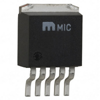
MIC39500-1.8BU
Manufacturer Part Number
MIC39500-1.8BU
Description
IC REG LDO 5A 1.0% 1.8V TO-263
Manufacturer
Micrel Inc
Datasheet
1.MIC39500-1.8WU.pdf
(10 pages)
Specifications of MIC39500-1.8BU
Regulator Topology
Positive Fixed
Voltage - Output
1.8V
Voltage - Input
2.25 ~ 16 V
Voltage - Dropout (typical)
0.4V @ 5A
Number Of Regulators
1
Current - Output
5A (Min)
Operating Temperature
-40°C ~ 125°C
Mounting Type
Surface Mount
Package / Case
TO-263-3, D²Pak (3 leads + Tab), TO-263AA
Lead Free Status / RoHS Status
Contains lead / RoHS non-compliant
Current - Limit (min)
-
Available stocks
Company
Part Number
Manufacturer
Quantity
Price

Part Number:
MIC39500-1.8BU
Manufacturer:
MICREL
Quantity:
20 000


Absolute Maximum Ratings
Supply Voltage (V
Enable Voltage (V
Storage Temperature (T
Lead Temperature (soldering, 5 sec.) ........................ 260°C
ESD, Note 3
Electrical Characteristics
T
Symbol
Symbol
Symbol
Symbol
Symbol
Symbol
Symbol
V
∆V
ppm/°C
V
I
I
I
e
µV(rms)
Enable Input (MIC39501)
V
I
I
Flag Output (MIC39501)
I
V
V
Note 1.
Note 2.
Note 3.
Note 4.
Note 5.
Note 6.
Note 7.
Note 8.
Note 9.
August 2005
MIC39500/39501
GND
GND(do)
OUT(lim)
IN
OUT(shdn)
FLG(leak)
n
J
OUT
DO
EN
FLG(do)
FLG
= 25°C, bold values indicate –40°C ≤ T
OUT
/∆T
/∆T
Exceeding the absolute maximum ratings may damage the device.
The device is not guaranteed to function outside its operating rating.
Devices are ESD sensitive. Handling precautions recommended.
P
Output voltage temperature coeffi cient is ∆V
V
age is the input-to-output voltage differential with the minimum input voltage being 2.25V. Minimum input operating voltage is 2.25V.
I
V
For a 2.5V device, V
GND
D(max)
DO
EN
≤ 0.8V, V
= V
is the quiescent current. I
Parameter
Parameter
Parameter
Parameter
Parameter
Parameter
Parameter
Output Voltage
Output Voltage
Output Voltage
Line Regulation
Line Regulation
Load Regulation
Load Regulation
Load Regulation
Output Voltage Temp. Coeffi cient,
Output Voltage Temp. Coeffi cient,
Note 5
Dropout Voltage, Note 6
Dropout Voltage,
Ground Current, Note 7
Ground Current,
Dropout Ground Pin Current
Dropout Ground Pin Current
Dropout Ground Pin Current
Current Limit
Current Limit
Current Limit
Output Noise Voltage
Output Noise Voltage
Output Noise Voltage
Enable Input Voltage
Enable Input Voltage
Enable Input Voltage
Enable Input Voltage
Enable Input Voltage
Enable Input Current
Enable Input Current
Enable Input Current
Shutdown Output Current
Shutdown Output Current
Output Leakage Current
Output Leakage Current
Output Leakage Current
Output Low Voltage
Output Low Voltage
Output Low Voltage
Low Threshold
Low Threshold
High Threshold
High Threshold
High Threshold
Hysteresis
Hysteresis
Hysteresis
Hysteresis
Hysteresis
Hysteresis
Hysteresis
= (T
IN
– V
J(max)
IN
EN
IN
OUT
) .......................................–20V to +20V
) .................................................. +20V
≤ 8V, and V
– T
– T
– T ) ÷ θ
when V
S
IN
) ........................ –65°C to +150°C
A
A
= 2.250V (device is in dropout).
OUT
JA
OUT
, where θ
decreases to 98% of its nominal output voltage with V
IN
= 0V
= I
GND
J
JA
JA
JA
(Note 1)
≤ +125°C; unless noted
+ I
depends upon the printed circuit layout. See “Applications Information.”
depends upon the printed circuit layout. See “Applications Information.”
OUT
OUT(worst case)
.
Condition
Condition
Condition
Condition
Condition
Condition
Condition
10mA
10mA
10mA
10mA ≤ I
I
I
V
V
V
I
I
I
I
I
I
I
I
I
I
I
I
V
V
V
V
V
V
C
C
C
logic low (off)
logic low (off)
logic low (off)
logic low (off)
logic low (off)
logic high (on)
logic high (on)
logic high (on)
V
V
V
V
V
V
Note 8
V
V
V
V
V
V
1% of V
1% of V
1% of V
1% of V
1% of V
OUT
OUT
OUT
OUT
OUT
OUT
IN
IN
OUT
EN
EN
OH
IN
OUT
= V
≤ V
= 2.250V, I
= V
= 0.8V
= 0.8V
= 0.8V
= 0.8V
= 0.8V
= 16V
= 16V
= 16V
= 16V
= 16V
= 10mA, V
= 250mA, ∆V
= 2.5A, ∆V
= 5A, ∆V
= 2.5A, V
= 5A, V
= 0V, V
= 47µF, I
÷ (T
OUT
OUT(nominal)
OUT
OUT
OUT
OUT
IN
OUT
J(max)
+ 1V, 10mA ≤ I
IN
3
IN
≤ 5A, V
OUT
IN
OL
OUT
= V
OUT
= V
Operating Ratings
Supply Voltage (V
Enable Voltage (V
Maximum Power Dissipation (P
Junction Temperature (T
Package Thermal Resistance
OUT
– T
= V
, = 250µA, Note 9
OUT
= –2%
= –2%
= –2%
OUT
TO-263 (θ
TO-220 (θ
J(min)
OUT
= 100mA, 10Hz to 100kHz
= 100mA, 10Hz to 100kHz
= 100mA, 10Hz to 100kHz
= 100mA, 10Hz to 100kHz
– 0.5V, I
+ 1V ≤ V
= –2%
= –2%
= –2%
= –2%
= –2%
OUT
OUT
= –2%
= –2%
= –2%
+ 1V
+ 1V
+ 1V
+ 1V
+ 1V
) where T
+ 1V
+ 1V
+ 1V
+ 1V
+ 1V
+ 1V
+ 1V
+ 1V
+ 1V ≤ V
OUT
OUT
IN
IN
JC
JC
≤ 5A
≤ 5A
≤ 5A
≤ 5A
≤ 5A
≤ 16V
≤ 16V
≤ 16V
≤ 16V
≤ 16V
J(max)
= V
= 10mA
= 10mA
= 10mA
= 10mA
= 10mA
) ......................................................... 2°C/W
) ......................................................... 2°C/W
IN
OUT
IN
EN
≤ 16V
is +125°C and T
) ................................... +2.25V to +16V
) .................................................. +16V
+ 1V. For voltages below 2.25V, Dropout volt-
J
) ........................ –40°C to +125°C
(Note 2)
2.25
Min
Min
Min
Min
Min
Min
Min
–1
–2
–2
93
93
93
93
1
1
1
D(max)
J(min)
is –40°C.
) ..................... Note 4
0.06
0.06
0.06
0.06
0.06
0.01
0.01
0.01
0.01
0.01
Typ
Typ
Typ
Typ
Typ
Typ
Typ
125
125
125
320
320
320
320
320
400
400
400
260
260
260
260
180
180
180
180
180
0.2
0.2
0.2
0.2
0.2
2.1
2.1
2.1
2.1
2.1
7.5
7.5
7.5
7.5
7.5
20
20
20
20
15
15
15
70
70
70
70
70
30
30
30
30
30
10
10
10
1
1
1
1
1
1
1
M9999-082605-B
Max
Max
Max
Max
Max
Max
Max
99.2
99.2
100
100
100
100
250
575
300
300
300
300
300
400
0.5
0.5
0.5
0.5
0.5
0.8
50
35
35
35
35
35
75
20
1
1
1
1
2
1
1
1
1
1
2
2
2
2
2
4
1
1
1
1
1
2
Micrel
Units
Units
Units
Units
Units
Units
Units
mV
mV
mV
mV
mV
mV
mV
mV
mV
mV
mV
mV
mV
mV
mA
mA
mA
mA
mA
mA
mA
mA
mA
mA
mA
µA
µA
µA
µA
µA
µA
µA
µA
µA
µA
µA
µA
µA
µA
µA
µA
µA
µA
µA
µA
µA
%
%
%
%
%
%
%
%
%
%
%
%
%
%
%
%
%
%
%
%
%
%
%
%
%
%
%
%
%
V
V
A
A
A
A
A
Related parts for MIC39500-1.8BU
Image
Part Number
Description
Manufacturer
Datasheet
Request
R

Part Number:
Description:
IC REG LDO 5A 1.0% 1.8V TO220-3
Manufacturer:
Micrel Inc
Datasheet:
Part Number:
Description:
IC REG LDO 5A 1.0% 2.5V TO220-3
Manufacturer:
Micrel Inc
Datasheet:

Part Number:
Description:
IC REG LDO 5A 1.0% 1.8V TO-263
Manufacturer:
Micrel Inc
Datasheet:
Part Number:
Description:
IC REG LDO 5A 1.0% 2.5V TO-263
Manufacturer:
Micrel Inc
Datasheet:
Part Number:
Description:
5.0A 1.0% Fixed Voltage LDO( )
Manufacturer:
Micrel Inc
Datasheet:
Part Number:
Description:
5.0A 1.0% Fixed Voltage LDO( )
Manufacturer:
Micrel Inc
Datasheet:
Part Number:
Description:
5.0A 1.0% Fixed Voltage LDO( )
Manufacturer:
Micrel Inc
Datasheet:
Part Number:
Description:
5.0A 1.0% Fixed Voltage LDO( )
Manufacturer:
Micrel Inc
Datasheet:

Part Number:
Description:
IC REG LDO 5.0A 2.5V TO263
Manufacturer:
Micrel Inc
Datasheet:
Part Number:
Description:
IC,VOLT REGULATOR,FIXED,+2.5V,BIPOLAR,SIP,3PIN,PLASTIC
Manufacturer:
Micrel Inc
Datasheet:
Part Number:
Description:
5.0A 1.0% Fixed Voltage LDO( )
Manufacturer:
Micrel Inc
Datasheet:

Part Number:
Description:
Manufacturer:
Micrel Inc
Datasheet:
Part Number:
Description:
Manufacturer:
Micrel Inc
Datasheet:
Part Number:
Description:
Manufacturer:
Micrel Inc
Datasheet:
Part Number:
Description:
Manufacturer:
Micrel Inc
Datasheet: