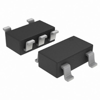
NCP511SN25T1G ON Semiconductor, NCP511SN25T1G Datasheet - Page 9

NCP511SN25T1G
Manufacturer Part Number
NCP511SN25T1G
Description
IC REG LDO 150MA 2.5V SOT23-5
Manufacturer
ON Semiconductor
Datasheet
1.NCP511SN33T1G.pdf
(11 pages)
Specifications of NCP511SN25T1G
Regulator Topology
Positive Fixed
Voltage - Output
2.5V
Voltage - Input
Up to 6V
Voltage - Dropout (typical)
0.11V @ 100mA
Number Of Regulators
1
Current - Output
150mA (Min)
Operating Temperature
-40°C ~ 85°C
Mounting Type
Surface Mount
Package / Case
TSOT-23-5, TSOT-5, TSOP-5
Number Of Outputs
1
Polarity
Positive
Input Voltage Max
6 V
Output Voltage
2.5 V
Output Type
Fixed
Dropout Voltage (max)
0.2 V at 100 mA
Output Current
150 mA
Line Regulation
3.5 mV / V
Load Regulation
0.8 mV / mA
Voltage Regulation Accuracy
2 %
Maximum Operating Temperature
+ 85 C
Mounting Style
SMD/SMT
Minimum Operating Temperature
- 40 C
Lead Free Status / RoHS Status
Lead free / RoHS Compliant
Current - Limit (min)
-
Lead Free Status / Rohs Status
Details
Other names
NCP511SN25T1GOSTR
Available stocks
Company
Part Number
Manufacturer
Quantity
Price
Company:
Part Number:
NCP511SN25T1G
Manufacturer:
ONSemico
Quantity:
16 950
Company:
Part Number:
NCP511SN25T1G
Manufacturer:
ON Semiconductor
Quantity:
7 200
Part Number:
NCP511SN25T1G
Manufacturer:
ON/安森美
Quantity:
20 000
Input
Enable
The NCP511 series can be current boosted with a PNP transist‐
or. Resistor R in conjunction with V
when the pass transistor begins conducting; this circuit is not
short circuit proof. Input/Output differential voltage minimum is
increased by V
If a delayed turn-on is needed during power up of several
voltages then the above schematic can be used. Resistor R,
and capacitor C, will delay the turn-on of the bottom regulator.
A few values were chosen and the resulting delay can be seen
in Figure 21.
R
1.0 mF
Input
Figure 18. Current Boost Regulator
Q1
Figure 20. Delayed Turn-on
BE
R
of the pass resistor.
1.0 mF
1.0 mF
C
1
2
3
1
2
3
1
2
3
Input
BE
R
A regulated output can be achieved with input voltages that
exceed the 6.0 V maximum rating of the NCP511 series with
the addition of a simple pre-regulator circuit. Care must be
taken to prevent Q1 from overheating when the regulated
output (V
of the PNP determines
5.6 V
Figure 22. Input Voltages Greater than 6.0 V
5
4
5
4
5
4
out
Q1
) is shorted to GND.
1.0 mF
1.0 mF
APPLICATION CIRCUITS
Output
1.0 mF
1.0 mF
Output
Output
http://onsemi.com
Input
NCP511
Q2
9
Short circuit current limit is essentially set by the V
R1. I
1
2
3
4
3
2
1
0
3
2
1
0
R1
R2
0
0
SC
The graph shows the delay between the enable signal and
output turn-on for various resistor and capacitor values.
= ((V
Figure 19. Current Boost Regulator
20
20
BEQ2
1.0 mF
R3
5
4
with Short Circuit Limit
No Delay
No Delay
Figure 21. Delayed Turn-on
40
40
- ib * R2) / R1) + I
R = 1.0 MW
R = 1.0 mW
C = 0.1 mF
C = 0.1 mF
Q1
1.0 mF
60
60
Output
Time (ms)
Time (ms)
1
2
3
80
80
O(max) Regulator
R = 1.0 MW
R = 1.0 MW
C = 1.0 mF
C = 1.0 mF
100
100
T
V
V
A
out
in
120
120
5
4
= 25°C
= 3.5 V
BE
= 3.0 V
of Q2 and
140
140
1.0 mF
Output
160
160


