NCP1117ST12T3 ON Semiconductor, NCP1117ST12T3 Datasheet - Page 3
NCP1117ST12T3
Manufacturer Part Number
NCP1117ST12T3
Description
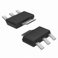
IC REG LDO 1A 12.0V SOT223
Manufacturer
ON Semiconductor
Datasheet
1.NCV1117ST50T3G.pdf
(18 pages)
Specifications of NCP1117ST12T3
Regulator Topology
Positive Fixed
Voltage - Output
12V
Voltage - Input
Up to 20V
Voltage - Dropout (typical)
1.07V @ 800mA
Number Of Regulators
1
Current - Limit (min)
1A
Operating Temperature
0°C ~ 125°C
Mounting Type
Surface Mount
Package / Case
SOT-223 (3 leads + Tab), SC-73, TO-261
Lead Free Status / RoHS Status
Contains lead / RoHS non-compliant
Current - Output
-
Other names
NCP1117ST12T3OS


4. NCP1117: T
5. Low duty cycle pulse techniques are used during testing to maintain the junction temperature as close to ambient as possible.
ELECTRICAL CHARACTERISTICS
operating ambient temperature range that applies unless otherwise noted. (Note 4)
Reference Voltage, Adjustable Output Devices
Output Voltage, Fixed Output Devices
Line Regulation (Note 5)
Load Regulation (Note 5)
NCV1117: T
(V
(V
1.5 V
1.8 V
1.9 V
2.0 V
2.5 V
2.85 V
3.3 V
5.0 V
12 V
1.5 V
1.8 V
1.9 V
2.0 V
2.5 V
2.85 V
3.3 V
5.0 V
12 V
1.5 V
1.8 V
1.9 V
2.0 V
2.5 V
2.85 V
3.3 V
5.0 V
12 V
in
in
–V
–V
low
low
out
out
= 0°C ,
= −40°C, T
= 2.0 V, I
= 1.4 V to 10 V, I
(V
(V
(V
(V
(V
(V
(V
(V
(V
(V
(V
(V
(V
(V
(V
(V
(V
(V
(V
(V
(V
(V
(V
(V
(V
(V
(V
(V
(I
(I
(I
(I
(I
(I
(I
(I
(I
out
out
out
out
out
out
out
out
out
in
in
in
in
in
in
in
in
in
in
in
in
in
in
in
in
in
in
in
in
in
in
in
in
in
in
in
in
= 3.5 V, I
= 2.9 V to 11.5 V, I
= 3.8 V, I
= 3.2 V to 11.8 V, I
= 3.9 V, I
= 3.3 V to 11.9 V, I
= 4.0 V, I
= 3.4 V to 12 V, I
= 4.5 V, I
= 3.9 V to 10 V, I
= 4.85 V, I
= 4.25 V to 10 V, I
= 4.0 V, I
= 5.3 V, I
= 4.75 V to 10 V, I
= 7.0 V, I
= 6.5 V to 12 V, I
= 14 V, I
= 13.5 V to 20 V, I
= 2.9 V to 11.5 V, I
= 3.2 V to 11.8 V, I
= 3.3 V to 11.9 V, I
= 3.4 V to 12 V, I
= 3.9 V to 10 V, I
= 4.25 V to 10 V, I
= 4.75 V to 15 V, I
= 6.5 V to 15 V, I
= 13.5 V to 20 V, I
= 0 mA to 800 mA, V
= 0 mA to 800 mA, V
= 0 mA to 800 mA, V
= 0 mA to 800 mA, V
= 0 mA to 800 mA, V
= 0 mA to 800 mA, V
= 0 mA to 800 mA, V
= 0 mA to 800 mA, V
= 0 mA to 800 mA, V
T
out
high
high
Adjustable (V
Adjustable (I
= 10 mA, T
out
= 125°C
= 125°C
out
out
out
out
out
out
out
out
Characteristic
out
= 10 mA, T
out
= 10 mA, T
= 10 mA, T
= 10 mA, T
= 10 mA, T
= 10 mA, T
= 0 mA to 500 mA) (Note 4)
= 10 mA, T
= 10 mA, T
= 10 mA, T
= 10 mA to 800 mA) (Note 4)
out
out
out
out
out
out
(C
A
out
out
out
out
out
out
out
out
out
out
out
out
out
in
in
= 0 mA to 800 mA) (Note 4)
= 0 mA to 800 mA,) (Note 4)
= 0 mA to 800 mA) (Note 4)
= 0 mA)
= 0 mA)
= 0 mA)
= 25°C)
= 0 mA to 800 mA) (Note 4)
= 0 mA to 800 mA) (Note 4)
= 0 mA to 800 mA) (Note 4)
= 0 mA)
= 0 mA)
= 0 mA)
in
in
in
in
in
in
in
in
in
= 0 mA to 800 mA) (Note 4)
= 0 mA to 800 mA) (Note 4)
= 0 mA to 800 mA) (Note 4)
= 0 mA)
= 0 mA)
= 0 mA)
= 10 mF, C
= 2.75 V to 16.25 V, I
= 10 mA to 800 mA, V
A
A
A
A
A
A
A
A
= 2.9 V)
= 3.2 V)
= 3.3 V)
= 3.4 V)
= 3.9 V)
= 4.25 V)
= 4.75 V)
= 6.5 V)
= 13.5 V)
= 25 °C)
A
= 25 °C)
= 25 °C)
= 25 °C)
= 25 °C)
= 25 °C)
= 25 °C)
= 25 °C)
= 25 °C)
out
http://onsemi.com
= 10 mF, for typical value T
out
3
in
= 10 mA)
= 4.25 V)
A
Symbol
= 25°C, for min and max values T
Reg
Reg
V
V
out
ref
line
line
11.880
11.760
1.238
1.225
1.485
1.470
1.782
1.755
1.872
1.862
1.970
1.960
2.475
2.450
2.821
2.790
2.790
3.267
3.235
4.950
4.900
Min
−
−
−
−
−
−
−
−
−
−
−
−
−
−
−
−
−
−
−
−
12.000
1.500
1.800
1.900
1.900
2.000
2.500
2.850
3.300
5.000
1.25
0.04
Typ
0.3
0.4
0.5
0.5
0.5
0.8
0.8
0.9
1.0
0.2
2.3
2.6
2.7
3.0
3.3
3.8
4.3
6.7
16
−
−
−
−
−
−
−
−
−
−
12.120
12.240
1.262
1.270
1.515
1.530
1.818
1.845
1.929
1.938
2.030
2.040
2.525
2.550
2.879
2.910
2.910
3.333
3.365
5.050
5.100
Max
A
0.1
1.0
1.0
2.5
2.5
2.5
3.0
4.5
6.0
7.5
0.4
5.5
6.0
6.0
6.0
7.5
8.0
10
15
28
is the
Unit
mV
mV
%
%
V
V
Related parts for NCP1117ST12T3
Image
Part Number
Description
Manufacturer
Datasheet
Request
R

Part Number:
Description:
1.0 A Low−Dropout Positive Fixed and Adjustable Voltage Regulators
Manufacturer:
ONSEMI [ON Semiconductor]
Datasheet:

Part Number:
Description:
ON Semiconductor [VOLTAGE REGULATOR]
Manufacturer:
ON Semiconductor
Datasheet:
Part Number:
Description:
357-036-542-201 CARDEDGE 36POS DL .156 BLK LOPRO
Manufacturer:
ON Semiconductor
Datasheet:
Part Number:
Description:
357-036-542-201 CARDEDGE 36POS DL .156 BLK LOPRO
Manufacturer:
ON Semiconductor
Datasheet:
Part Number:
Description:
357-036-542-201 CARDEDGE 36POS DL .156 BLK LOPRO
Manufacturer:
ON Semiconductor
Datasheet:
Part Number:
Description:
357-036-542-201 CARDEDGE 36POS DL .156 BLK LOPRO
Manufacturer:
ON Semiconductor
Datasheet:
Part Number:
Description:
357-036-542-201 CARDEDGE 36POS DL .156 BLK LOPRO
Manufacturer:
ON Semiconductor
Datasheet:
Part Number:
Description:
357-036-542-201 CARDEDGE 36POS DL .156 BLK LOPRO
Manufacturer:
ON Semiconductor
Datasheet:
Part Number:
Description:
357-036-542-201 CARDEDGE 36POS DL .156 BLK LOPRO
Manufacturer:
ON Semiconductor
Datasheet:
Part Number:
Description:
357-036-542-201 CARDEDGE 36POS DL .156 BLK LOPRO
Manufacturer:
ON Semiconductor
Datasheet:
Part Number:
Description:
357-036-542-201 CARDEDGE 36POS DL .156 BLK LOPRO
Manufacturer:
ON Semiconductor
Datasheet:
Part Number:
Description:
357-036-542-201 CARDEDGE 36POS DL .156 BLK LOPRO
Manufacturer:
ON Semiconductor
Datasheet:
Part Number:
Description:
Manufacturer:
ON Semiconductor
Datasheet: