CAT6221-SGTD-GT3 ON Semiconductor, CAT6221-SGTD-GT3 Datasheet
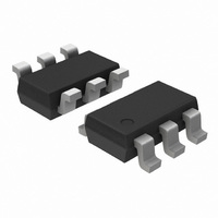
IC REG LDO .3A 3.3/1.8V TSOT23-6

CAT6221-SGTD-GT3

Manufacturer Part Number
CAT6221-SGTD-GT3
Description
IC REG LDO .3A 3.3/1.8V TSOT23-6
Manufacturer
ON Semiconductor
Datasheet

Specifications of CAT6221-SGTD-GT3

Regulator Topology
Positive Fixed
Voltage - Output
3.3V, 1.8V
Voltage - Input
2.3 ~ 5.5 V
Voltage - Dropout (typical)
0.21V @ 300mA
Number Of Regulators
2
Current - Output
300mA
Operating Temperature
-40°C ~ 125°C
Mounting Type
Surface Mount
Package / Case
TSOT-23-6, TSOT-6
Number Of Outputs
2
Polarity
Positive
Input Voltage Max
5.5 V
Output Voltage
3.3 V or 1.8 V
Output Type
Fixed
Dropout Voltage (max)
0.28 V at 300 mA
Output Current
0.3 A
Line Regulation
0.2 %/V
Load Regulation
1.5 %
Voltage Regulation Accuracy
1 %
Maximum Operating Temperature
+ 125 C
Mounting Style
SMD/SMT
Minimum Operating Temperature
- 40 C
Lead Free Status / RoHS Status
Lead free / RoHS Compliant
Current - Limit (min)
-
Lead Free Status / Rohs Status
Lead free / RoHS Compliant
Other names
CAT6221-SGTD-GT3CT

Available stocks

Company
Part Number
Manufacturer
Quantity
Price
Part Number:
CAT6221-SGTD-GT3
Manufacturer:
ON Semiconductor
Quantity:
1 650
CAT6221
300 mA CMOS Dual LDO
Regulator
Description
TSOT−23 6−lead package two low dropout regulators (LDO), each
with its own enable pin.
LDO provides fast response time during load current and line voltage
changes.
With zero shut down current and a low quiescent current of 100 mA,
the dual LDO is ideal for battery−operated devices with supply voltage
from 2.3 V to 5.5 V.
voltage, typical 210 mV at 300 mA. Stable operation is provided with
small 1 mF ceramic output capacitors, reducing required board space
and component cost.
protection.
with a maximum height of 0.8 mm.
Features
Applications
© Semiconductor Components Industries, LLC, 2011
February, 2011 − Rev. 2
The 300 mA CMOS Dual LDO CAT6221 combines in a single
The regulator outputs drive loads up to 300 mA. By design, the dual
Each LDO is optimized for low noise and high crosstalk isolation.
The dual LDO offers 1% initial accuracy and very low dropout
Other features include fold−back current limit and thermal
The dual LDO is available in the tiny 6−lead TSOT−23 package
Compliant
Two Outputs with Guaranteed 300 mA Peak Output Current
Low Dropout Voltages of 210 mV Typical at 300 mA
Stable with Ceramic Output Capacitors
Independent Enable Pins
Under Voltage Lockout
No−load Ground Current of 100 mA Typical
Full−load Ground Current of 160 mA Typical
±1.0% Output Voltage Initial Accuracy (V
±2.0% Accuracy Over Temperature (V
“Zero” Current Shutdown Mode
Fold−back Current Limit and Thermal Protection
TSOT−23 6−lead, 0.8 mm Height Package
These Devices are Pb−Free, Halogen Free/BFR Free and are RoHS
Cellular Phones
Battery−powered Devices
Consumer Electronics
OUT
OUT
≥ 2.0 V)
≥ 2.0 V)
1
See detailed ordering and shipping information in the package
dimensions section on page 10 of this data sheet.
Pin #
1
2
3
4
5
6
T3 = CAT6221 Device Code
Y = Production Year (last digit)
M = Production Month: 1 − 9, A, B, C
VOUT2
VOUT1
Name
ORDERING INFORMATION
GND
EN1
EN2
VIN
EN1
EN2
VIN
MARKING DIAGRAM
PIN CONNECTIONS
http://onsemi.com
PIN FUNCTION
CASE 419AF
Enable input (active high) for
VOUT1.
Supply voltage input.
Enable input (active high) for
VOUT2.
LDO Output Voltage 2.
Ground reference.
LDO Output Voltage 1.
1
6
TD SUFFIX
(Top View)
TSOT−23
T3YM
Publication Order Number:
1
Function
VOUT1
GND
VOUT2
CAT6221/D

Related parts for CAT6221-SGTD-GT3

CAT6221-SGTD-GT3 Summary of contents

Page 1

... CMOS Dual LDO Regulator Description The 300 mA CMOS Dual LDO CAT6221 combines in a single TSOT−23 6−lead package two low dropout regulators (LDO), each with its own enable pin. The regulator outputs drive loads up to 300 mA. By design, the dual LDO provides fast response time during load current and line voltage changes ...

Page 2

... OUT1 1 mF EN2 VOUT2 C OUT2 1 mF Figure 2. CAT6221 Functional Block Diagram pins and ground. For better transient response, its value can be increased to 4.7 mF. pin and ground IN The capacitor should be located near the device. For the TSOT23 6−lead package, a continuous 300 mA output current for both LDOs may turn− ...

Page 3

Table 3. ELECTRICAL OPERATING CHARACTERISTICS ( 1 High 100 mA OUT EN OUT conditions unless specified otherwise). Bold numbers apply for the entire junction temperature range.) Symbol Parameter V Output ...

Page 4

TYPICAL CHARACTERISTICS ( 100 mA, EN1 = EN2 = V IN OUT Figure 3. Output Voltage 1 vs. Temperature Figure 5. Load Regulation VOUT1 Figure 7. Ground Current (EN2 = GND) (shown for 2.8 V/1.8 ...

Page 5

TYPICAL CHARACTERISTICS ( 100 mA, EN1 = EN2 = V IN OUT Figure 9. Ground Current (EN2 = GND) Figure 11. Output 1 Dropout Characteristics Figure 13. Output Voltage 1 vs. Load Current 1 (shown ...

Page 6

TYPICAL CHARACTERISTICS ( 100 mA, EN1 = EN2 = V IN OUT Figure 15. Line Regulation VOUT1 Figure 17. PSRR 1 & 2 vs. Frequency http://onsemi.com (shown for 2.8 V/1.8 V outputs option ...

Page 7

TRANSIENT CHARACTERISTICS ( 100 mA, EN1 = EN2 = V IN OUT Figure 18. Enable Turn−on (100 mA Loads) Figure 20. Enable Turn−on (300 mA/100 mA Loads) Figure 22. Enable Turn−on (100 mA/300 mA Loads) ...

Page 8

TRANSIENT CHARACTERISTICS ( 100 mA, EN1 = EN2 = V IN OUT Figure 24. VOUT1 Load Transient Response (0.1 to 300 mA) Figure 26. Line Transient Response (0.1 mA Loads) Figure 28. Line Transient Response ...

Page 9

TOP VIEW SIDE VIEW Notes: (1) All dimensions are in millimeters. Angles in degrees. (2) Complies with JEDEC MO-193. PACKAGE DIMENSIONS TSOT−23, 6 LEAD CASE 419AF−01 ISSUE O SYMBOL MIN A A1 0.01 A2 ...

Page 10

... All packages are RoHS−compliant (Lead−free, Halogen−free). 8. The standard finish is NiPdAu pre−plated (PPF) lead frames. 9. The device used in the above example is a CAT6221−MGTD−GT3 (V & Reel). 10. For other voltage options, please contact your nearest ON Semiconductor Sales office. ...

Related keywords