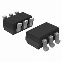
NUP2202W1T2G ON Semiconductor, NUP2202W1T2G Datasheet - Page 2

NUP2202W1T2G
Manufacturer Part Number
NUP2202W1T2G
Description
IC DIODE/TVS ARRAY HS SOT-363
Manufacturer
ON Semiconductor
Datasheet
1.NUP2202W1T2G.pdf
(8 pages)
Specifications of NUP2202W1T2G
Voltage - Reverse Standoff (typ)
5V
Voltage - Breakdown
6V
Power (watts)
500W
Polarization
2 Channel Array - Bidirectional
Mounting Type
Surface Mount
Package / Case
SC-70-6, SC-88, SOT-363
Applications
General Purpose
Number Of Circuits
2
Voltage - Working
5V
Voltage - Clamping
20V
Technology
Diode Array
Polarity
Unidirectional
Channels
1 Channel
Clamping Voltage
20 V
Operating Voltage
5 V
Breakdown Voltage
6 V
Termination Style
SMD/SMT
Peak Surge Current
28 A
Peak Pulse Power Dissipation
500 W
Capacitance
3 pF
Maximum Operating Temperature
+ 125 C
Minimum Operating Temperature
- 40 C
Dimensions
1.25 mm W x 2 mm L
Lead Free Status / RoHS Status
Lead free / RoHS Compliant
Other names
NUP2202W1T2G
NUP2202W1T2GOSTR
NUP2202W1T2GOSTR
Available stocks
Company
Part Number
Manufacturer
Quantity
Price
Company:
Part Number:
NUP2202W1T2G
Manufacturer:
ON
Quantity:
3 000
Company:
Part Number:
NUP2202W1T2G
Manufacturer:
ON
Quantity:
30 000
Company:
Part Number:
NUP2202W1T2G
Manufacturer:
OSRAM
Quantity:
5 740
Part Number:
NUP2202W1T2G
Manufacturer:
ON/安森美
Quantity:
20 000
ELECTRICAL CHARACTERISTICS
(T
*See Application Note AND8308/D for detailed explanations of
ELECTRICAL CHARACTERISTICS
2. TVS devices are normally selected according to the working peak reverse voltage (V
3. V
4. Nonrepetitive current pulse per Figure 5 (Pin 5 to Pin 2).
5. Surge current waveform per Figure 5.
6. For test procedure see Figures 3 and 4 and Application Note AND8307/D.
Reverse Working Voltage
Breakdown Voltage
Reverse Leakage Current
Clamping Voltage
Clamping Voltage
Maximum Peak Pulse Current
Junction Capacitance
Junction Capacitance
Clamping Voltage
Symbol
A
datasheet parameters.
V
V
P
= 25°C unless otherwise noted)
I
RWM
V
V
or continuous peak operating voltage level.
I
PP
I
I
C
BR
R
T
F
pk
C
F
BR
Figure 1. ESD Clamping Voltage Screenshot
is measured at pulse test current I
Positive 8 kV Contact per IEC61000−4−2
Parameter
Maximum Reverse Peak Pulse Current
Clamping Voltage @ I
Working Peak Reverse Voltage
Maximum Reverse Leakage Current @ V
Breakdown Voltage @ I
Test Current
Forward Current
Forward Voltage @ I
Peak Power Dissipation
Capacitance @ V
R
= 0 and f = 1.0 MHz
Parameter
F
PP
Symbol
V
T
V
RWM
I
V
V
V
C
C
I
PP
BR
R
C
C
C
J
J
(T
T
.
J
=25°C unless otherwise specified)
(Note 2)
I
V
I
I
8x20 ms Waveform (Note 4)
V
V
Per IEC 61000−4−2 (Note 6)
T
PP
PP
RWM
R
R
= 1 mA, (Note 3)
= 0 V, f = 1 MHz between I/O Pins and GND
= 0 V, f = 1 MHz between I/O Pins
= 5 A (Note 4)
= 8 A (Note 4)
= 5 V
RWM
http://onsemi.com
Conditions
2
Figure 2. ESD Clamping Voltage Screenshot
Negative 8 kV Contact per IEC61000−4−2
V
C
V
RWM
BR
V
), which should be equal or greater than the DC
RWM
Uni−Directional TVS
Min
6.0
I
F
I
I
I
I
R
T
PP
Figure 1 and 2
V
F
Typ
8.5
8.9
3.0
1.5
Max
12.5
5.0
5.0
5.0
3.0
20
28
V
Unit
mA
pF
pF
V
V
V
V
A
V


