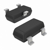
SL15T1 ON Semiconductor, SL15T1 Datasheet - Page 2

SL15T1
Manufacturer Part Number
SL15T1
Description
TVS LO CAP 300W 15V ESD SOT23
Manufacturer
ON Semiconductor
Specifications of SL15T1
Voltage - Reverse Standoff (typ)
15V
Voltage - Breakdown
16.7V
Power (watts)
300W
Polarization
Bidirectional
Mounting Type
Surface Mount
Package / Case
SOT-23-3, TO-236-3, Micro3™, SSD3, SST3
Applications
General Purpose
Number Of Circuits
1
Voltage - Working
15V
Voltage - Clamping
24V
Technology
Diode Array
Lead Free Status / RoHS Status
Contains lead / RoHS non-compliant
Other names
SL15T1OS
Available stocks
Company
Part Number
Manufacturer
Quantity
Price
Company:
Part Number:
SL15T1
Manufacturer:
ON Semiconductor
Quantity:
75
Part Number:
SL15T1
Manufacturer:
ON/安森美
Quantity:
20 000
Company:
Part Number:
SL15T1G
Manufacturer:
ON Semiconductor
Quantity:
60 703
Company:
Part Number:
SL15T1G
Manufacturer:
ON Semiconductor
Quantity:
94
Company:
Part Number:
SL15T1G
Manufacturer:
ON
Quantity:
30 000
Company:
Part Number:
SL15T1G
Manufacturer:
ON
Quantity:
30 000
Part Number:
SL15T1G
Manufacturer:
ON/安森美
Quantity:
20 000
Stresses exceeding Maximum Ratings may damage the device. Maximum Ratings are stress ratings only. Functional operation above the
Recommended Operating Conditions is not implied. Extended exposure to stresses above the Recommended Operating Conditions may affect
device reliability.
1. Non−repetitive current pulse per Figure 2
2. FR−5 = 1.0 x 0.75 x 0.62 in.
3. Alumina = 0.4 x 0.3 x 0.024 in., 99.5% alumina
ELECTRICAL CHARACTERISTICS
(T
UNIDIRECTIONAL
MAXIMUM RATINGS
Symbol
Peak Power Dissipation @ 8x20 usec (Note 1)
IEC 61000−4−2
IEC 61000−4−4
IEC 61000−4−5
Total Power Dissipation on FR−5 Board (Note 2) @ T
Thermal Resistance Junction to Ambient
Total Power Dissipation on Alumina Substrate (Note 3) @ T
Thermal Resistance Junction−to−Ambient
Junction and Storage Temperature Range
Lead Solder Temperature − Maximum (10 Second Duration)
A
V
QV
V
Z
Z
= 25°C unless otherwise noted)
I
RWM
I
V
V
@ T
Contact Discharge
Air Discharge
Derate above 25°C
Derate above 25°C
I
PP
I
I
ZK
BR
R
ZT
ZK
T
F
C
F
BR
L
≤ 25°C
Maximum Reverse Peak Pulse Current
Clamping Voltage @ I
Working Peak Reverse Voltage
Maximum Reverse Leakage Current @ V
Breakdown Voltage @ I
Test Current
Maximum Temperature Coefficient of V
Forward Current
Forward Voltage @ I
Maximum Zener Impedance @ I
Reverse Current
Maximum Zener Impedance @ I
(Circuit tied to Pins 1 and 3 or 2 and 3)
Level 4
EFT
Lightning
Parameter
F
PP
T
Rating
ZT
ZK
BR
RWM
A
= 25°C
http://onsemi.com
SL05T1 Series
A
= 25°C
2
V
C
V
BR
V
RWM
Uni−Directional TVS
Symbol
T
°P
R
°P
R
J
P
V
, T
T
qJA
qJA
pk
pp
D
D
L
stg
°
°
I
F
I
I
I
I
R
T
PP
V
F
− 55 to +150
Value
300
±16
225
556
300
417
260
1.8
2.4
±8
40
12
mW/°C
mW/°C
V
°mW°
°C/W
°C/W
°mW
Unit
kV
kV
°C
°C
W
A
A


