NCP3712ASNT3 ON Semiconductor, NCP3712ASNT3 Datasheet
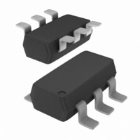
IC SWITCH OVP HIGH SIDE SC74-6

NCP3712ASNT3

Manufacturer Part Number
NCP3712ASNT3
Description
IC SWITCH OVP HIGH SIDE SC74-6
Manufacturer
ON Semiconductor
Datasheet

Specifications of NCP3712ASNT3

Technology
Mixed Technology
Power (watts)
300mW
Number Of Circuits
1
Applications
General Purpose
Package / Case
SC-74-6
Lead Free Status / RoHS Status
Contains lead / RoHS non-compliant
Voltage - Working
-
Voltage - Clamping
-
NCP3712ASN
Over Voltage Protected
High Side Switch
isolating the load from the transient energy rather than absorbing it.
Features
Applications Include:
© Semiconductor Components Industries, LLC, 2007
September, 2007 - Rev. 5
This switch is primarily intended to protect loads from transients by
Capable of Switching Loads of up to 200 mA without External
Switch Shuts Off in Response to an Over Voltage Input Transient
Features Active Turn Off for Fast Input Transient Protection
Flexible Over Voltage Protection Threshold Set with External Zener
Automatic Recovery after Transient Decays Below Threshold
Withstands Input Transients up to 105 V Peak
Guaranteed Off State with Enbl Input
ESD Resistant in Accordance with the 2000 V Human Body Model
Extremely Low Saturation Voltage
Pb-Free Packages are Available
High Voltage Transient Isolation
Power Switching to Electronic Modules
DC Power Distribution in Line Operated Equipment
Buffering Sensitive Circuits from Poorly Regulated Power Supplies
Pre-conditioning of Voltage Regulator Input Voltage
Rboost
P. S.
+
-
V
Figure 1. Typical Application Circuit
in
V
NCP3712ASN
Z
Enbl
1 k (min)
V
R
or
out
boost
SW
R
opt
O
A
D
L
1
†For information on tape and reel specifications,
NCP3712ASNT1
NCP3712ASNT1G
NCP3712ASNT3
NCP3712ASNT3G
including part orientation and tape sizes, please
refer to our Tape and Reel Packaging Specifications
Brochure, BRD8011/D.
N.C.
V
6
(5)
(2)
in
(Note: Microdot may be in either location)
Device
R2
1
(4)
INTERNAL CIRCUIT DIAGRAM/
ORDERING INFORMATION
BAG = Device Code
M
G
PIN CONFIGURATION
http://onsemi.com
V
R1
CASE 318F
Z
SC-74
= Date Code
= Pb-Free Package
(Pb-Free)
(Pb-Free)
Q1
Package
SC-74
SC-74
SC-74
SC-74
Publication Order Number:
R4
(1)
10,000/Tape & Reel
10,000/Tape & Reel
NCP3712ASNT1/D
3000/Tape & Reel
3000/Tape & Reel
Q2
MARKING
DIAGRAM
Shipping
BAG MG
R3
Enbl
G
V
(6)
R
(3)
out
boost

Related parts for NCP3712ASNT3

NCP3712ASNT3 Summary of contents

Page 1

... V (5) N.C. (2) R opt NCP3712ASNT1 NCP3712ASNT1G SW NCP3712ASNT3 NCP3712ASNT3G †For information on tape and reel specifications, including part orientation and tape sizes, please refer to our Tape and Reel Packaging Specifications Brochure, BRD8011/D. 1 http://onsemi.com MARKING DIAGRAM SC-74 BAG MG G CASE 318F 1 BAG = Device Code ...

Page 2

MAXIMUM RATINGS (T = 25°C unless otherwise noted) (Note 1) J Rating Input-to-Output Voltage Reverse Input-to-Vz. Voltage Reverse Input-to-Rboost Voltage Output Load Current - Continuous Enbl Input Current - Continuous Vz Input Current - Continuous Rboost Input Current - Continuous ...

Page 3

ELECTRICAL CHARACTERISTICS Characteristic OFF CHARACTERISTICS Input-Output Breakdown Voltage = 200 mA out Output Reverse Breakdown Voltage (@ I = -1.0 mA Pulse) out Output Leakage Current ( 25°C) in enbl A ...

Page 4

... Pb-Free strategy and soldering details, please download the ON Semiconductor Soldering and Mounting Techniques Reference Manual, SOLDERRM/D. ON Semiconductor and are registered trademarks of Semiconductor Components Industries, LLC (SCILLC). SCILLC reserves the right to make changes without further notice to any products herein ...

Related keywords