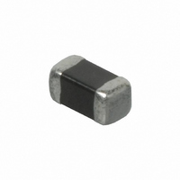
VR1005AAA270-T Taiyo Yuden, VR1005AAA270-T Datasheet - Page 7

VR1005AAA270-T
Manufacturer Part Number
VR1005AAA270-T
Description
VARISTOR 27V 40PF 0402 SMD
Manufacturer
Taiyo Yuden
Series
VRr
Datasheet
1.VR1005CCA270-T.pdf
(10 pages)
Specifications of VR1005AAA270-T
Varistor Voltage
27V
Current-surge
5A
Number Of Circuits
1
Maximum Dc Volts
15VDC
Package / Case
0402 (1005 Metric)
Lead Free Status / RoHS Status
Lead free / RoHS Compliant
Energy
-
Maximum Ac Volts
-
Other names
587-1419-2
NK VR 1005AAA270-T
NK VR 1005AAA270-T
Available stocks
Company
Part Number
Manufacturer
Quantity
Price
Company:
Part Number:
VR1005AAA270-T
Manufacturer:
MOLEX
Quantity:
32 207
Precautions on the use of Multilayer chip varistors.
△
!
PRECAUTIONS
1.Circuit Design
2.PCB Design
当社カタログをご使用の際には 「当社製品に関するお断り」 を必ずお読みください。
Stages
(Design of Land-patterns)
Verification of operating environment, electrical rating and
performance
1.A malfunction in medical equipment, spacecraft, nuclear
Operating Voltage (Verification of Rated voltage)
1.The operating voltage for varistors must always be lower
Pattern configurations
1.When varistors are mounted on a PCB, the amount of
(1) The amount of solder applied can affect the ability of
(2) When more than one part is jointly soldered onto the
reactors, etc. may cause serious harm to human life or have
severe social ramifications. As such, any varistors to be
used in such equipment may require higher safety and/or
reliability considerations and should be clearly differentiated
from components used in general purpose applications.
than their rated values.
If an AC voltage is loaded on a DC voltage, the sum of the
two peak voltages should be lower than the rated value of
the varistor chosen. For a circuit where both an AC and a
pulse voltage may be present, the sum of their peak
voltages shouldalso be lower than the varistor's rated
voltage.
solder used (size of fillet) can directly affect varistor
performance.
Therefore, the following items must be carefully considered
in the design of solder land patterns:
chips to withstand mechanical stresses which may lead
to breaking or cracking. Therefore, when designing
land-patterns it is necessary to consider the appropriate
size and configuration of the solder pads which in turn
determines the amount of solder necessary to form the
fillets.
same land or pad, the pad must be designed so that
each component's soldering point is separated by
solder-resist.
Precautions
1.The following diagrams and tables show some examples of recommended patterns
(1) Recommended land dimensions for a typical chip varistor land patterns for PCBs
(2) Examples of good and bad solder application
Mixed mounting
of SMD and
leaded
components
Component
placement close
to the chassis
Hand-soldering
of leaded
components
near mounted
components
Horizontal
component
placement
to prevent excessive solder amounts. (larger fillets which extend above the
component end terminations)
Examples of improper pattern designs are also shown.
Recommended land dimensions for reflow-soldering (unit: mm)
Size
Excess solder can affect the ability of chips to withstand mechanical stresses.
Therefore, please take proper precautions when designing land-patterns.
Items
Type
B
C
A
W
L
0.25∼0.40
Chip Varistor
0.2∼0.30
0.2∼0.30
0603
0.6
0.3
△
!
Not recommended
Please read the "Notice for TAIYO YUDEN products" before using this catalog.
Technical considerations
1005,105C
0.45∼0.55
0.40∼0.50
0.45∼055
1.0
0.5
Recommended
Chip Varistor
1/4
457
8


