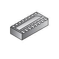
CM1235-08DE ON Semiconductor, CM1235-08DE Datasheet

CM1235-08DE
Specifications of CM1235-08DE
Available stocks
Related parts for CM1235-08DE
CM1235-08DE Summary of contents
Page 1
... The PicoGuard XS protection family is specifically designed for next generation deep sub-micron high speed data line protection. The CM1235 is ideal for protecting systems with high data and clock rates or for circuits requiring low capacitive loading and tightly controlled signal skews (with channel-to-channel matching at 2% max deviation) ...
Page 2
... Subsequent to the ESD/EOS event, both devices must immediately return to their original specifications, and be ready for an additional strike. Any deterioration in parasitics or clamping capability should be considered a failure, since it can then affect signal integrity or subsequent protection capability. (This is known as "multi- strike" capability.) Rev Page www.onsemi.com CM1235 ...
Page 3
... CM1235 In the CM1235 PicoGuard XS architecture, the signal line leading the connector to the ASIC routes through the CM1235 chip which provides 100Ω matched differential channel characteristic impedance that helps optimize 100Ω load impedance applications such as the HDMI high speed data lines. ...
Page 4
... ESD protection device. The inductor element represents the parasitic inductance arising from the bond wire and the PCB trace leading to the ESD protection diodes. Figure 3. CM1234 PicoGuard XS ESD Protection Model Figure 2. Standard ESD Protection Model Rev Page www.onsemi.com CM1235 ...
Page 5
... Each ESD channel consists of a pair of diodes in series that steer the positive or negative ESD current pulse to either the Zener diode or to ground. This embedded Zener diode also serves to eliminate the need for a separate bypass capacitor to absorb positive ESD strikes to ground. The CM1235 protects against ESD pulses up to ±8kV contact per the IEC 61000-4-2 standard. ...
Page 6
... Bidrectional Clamp to Connector (outside system) Bidrectional Clamp to Connector (outside system) Bidrectional Clamp to Connector (outside system) Bidrectional Clamp to Connector (outside system) Bidrectional Clamp to Connector (outside system) Bidrectional Clamp to Connector (outside system) Bidrectional Clamp to Connector (outside system) Rev Page www.onsemi.com CM1235 Description Ground return to shield ...
Page 7
... Breakdown Voltage (Positive) *Exposure to absolute maximum rating conditions for extended periods may affect device reliability. PART NUMBERING INFORMATION ORDERING PART NUMBER (LEAD-FREE FINISH) CM1235 ABSOLUTE MAXIMUM RATINGS* Rev Page www.onsemi.com PART MARKING -08DE CM1235 RATING -40 to +85 -65 to +150 6 UNITS ° C ° ...
Page 8
... TR = 200ps; Note 200ps; R Note 200ps 25º Note 2 = –40° +85° C unless otherwise noted. A uncompensated differential microstrip, with typical layout as Rev Page www.onsemi.com CM1235 (SEE NOTE 1) MIN TYP MAX UNITS -0.5 5.5 V 100 mA µA ±0.1 ±1.0 kV ±8 3 ...
Page 9
... CM1235 (PicoGuard XS ESD protector) lowers the peak voltage and clamping voltage by 45% across a wide range of loading conditions in comparison to a standard ESD protection device. indicates that the DUP/ASIC protected by the CM1235 dissipates less energy than a standard ESD protection device. This data was derived using the test setups shown in Figure 4 ...
Page 10
... Figure 6. Test Setups: Standard Device (Left) and CM1235 (Right) Figure 7. Typical Channel TDR Measured Across Out_x and In_x Per Each Differential Channels Pair (Typical 200ps Incident Rise Time) Rev Page www.onsemi.com CM1235 ...
Page 11
... CM1235 CM1235 Application and Guidelines As a general rule, the CM1235 ESD protection array should be located as close as possible to the point of entry of expected electrostatic discharges with minimum PCB trace lengths to the ground planes and between the sig- nal input and the ESD device to minimize stray series inductance. ...
Page 12
... Nom Max 0.028 0.030 0.031 0.000 0.001 0.002 0.008 0.010 0.012 0.153 0.157 0.161 0.124 0.126 0.128 0.063 0.067 0.071 0.018 0.020 0.022 0.020 BSC 0.012 REF 0.010 0.012 0.014 Rev Page www.onsemi.com CM1235 Dimensions for 16-Lead, 0.5mm pitch TDFN package ...
Page 13
... CM1235 Tape and Reel Specifications PACKAGE SIZE PART NUMBER (mm) CM1235 4.00 X 1.70 X 0.75 POCKET SIZE (mm) TAPE WIDTH 4.30 X 1.90 X 1.20 12mm Rev Page www.onsemi.com REEL QTY PER DIAMETER REEL 178mm (7") 3000 4mm 4mm 1 ...
Page 14
... N. American Technical Support: 800-282-9855 Toll Free USA/Canada Europe, Middle East and Africa Technical Support: Phone: 421 33 790 2910 Japan Customer Focus Center Phone: 81-3-5773-3850 Rev Page www.onsemi.com CM1235 ON Semiconductor Website: www.onsemi.com Order Literature: http://www.onsemi.com/orderlit For additional information, please contact your local Sales Representative ...


