UPC3223TB-EVAL CEL, UPC3223TB-EVAL Datasheet
UPC3223TB-EVAL
Specifications of UPC3223TB-EVAL


Related parts for UPC3223TB-EVAL


UPC3223TB-EVAL Summary of contents
Page 1
... Part number for sample order: Caution Observe precautions when handling because these devices are sensitive to electrostatic discharge. Document No. PU10491EJ01V0DS (1st edition) Date Published May 2004 CP(K) BIPOLAR ANALOG INTEGRATED CIRCUIT UPC3223TB 5 V, SILICON MMIC Marking • Embossed tape 8 mm wide C3J • ...
Page 2
... Remark Typical performance. Please refer to ELECTRICAL CHARACTERISTICS in detail. 2 (Bottom View Ω (dB) (dB) (mA) 15 6.5 26 6-pin super minimold 4.5 19 Data Sheet PU10491EJ01V0DS UPC3223TB Pin No. Pin Name 1 INPUT 2 GND 3 GND 4 OUTPUT 5 GND Package Marking C1D C1E C1F C2L C3J ...
Page 3
... This pin should be connected to system ground with minimum inductance. Ground pattern on the board should be formed as wide as possible. All the ground pins must be connected together with wide ground pattern to decrease impedance difference. = 5.0 V Data Sheet PU10491EJ01V0DS UPC3223TB and FE and output pins to supply CC 3 ...
Page 4
... GHz −30 dBm f = 1.0 GHz −30 dBm f = 2.2 GHz −30 dBm f = 1.0 GHz, P out in = −30 dBm f = 2.2 GHz 0.1 to 2.2 GHz P Data Sheet PU10491EJ01V0DS UPC3223TB Ratings Unit 6 270 mW −40 to +85 °C −55 to +150 °C +10 dBm MIN. TYP. MAX. Unit 4.5 5 ...
Page 5
... OTHER CHARACTERISTICS, FOR REFERENCE PURPOSES ONLY (T = +25° 5 out S Parameter Symbol Output Intercept Point OIP = 50 Ω Test Conditions f = 1.0 GHz 2.2 GHz Data Sheet PU10491EJ01V0DS UPC3223TB Reference Value Unit +17.8 dBm +14.8 5 ...
Page 6
... 100 100 Value 100 pF 1 000 pF 1 000 pF 100 nH pin (pin 6) and output pin (pin 4). Select large value inductance pin is used to minimize ground impedance Data Sheet PU10491EJ01V0DS UPC3223TB 50 Ω OUT pin and the coupling capacitors for CC pin. So, stable bias CC ...
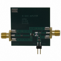
Page 7
... ILLUSTRATION OF THE TEST CIRCUIT ASSEMBLED ON EVALUATION BOARD IN C1 COMPONENT LIST Notes Value 100 000 100 × 30 × 0.4 mm double sided copper clad polyimide board. Back side: GND pattern Solder plated on pattern : Through holes Data Sheet PU10491EJ01V0DS UPC3223TB OUT 7 ...
Page 8
... OUTPUT RETURN LOSS vs. FREQUENCY 10 +25˚ 4 − 10 − 5.5 V − − 40 4.1 5.1 0.1 1.1 Data Sheet PU10491EJ01V0DS UPC3223TB +20 +40 +60 +80 +100 0 (° 5 2.1 3.1 4.1 5.1 Frequency f (GHz) = 5.0 V 2.1 3.1 4.1 5.1 Frequency f (GHz) ...
Page 9
... A − 10 − − T 40˚C A − 30 − 40 5.1 0.1 1.1 Frequency f (GHz) OUTPUT RETURN LOSS vs. FREQUENCY 5 − 10 − 20 − 30 − 40 5.1 0.1 1.1 Frequency f (GHz) Data Sheet PU10491EJ01V0DS UPC3223TB +25˚ 2.1 3.1 4.1 5.1 = − +85˚ 2.1 3.1 4.1 5.1 9 ...
Page 10
... INPUT POWER 5 200 MHz 201 MHz 2 5 − 10 − 20 − 30 − 40 − 50 − 60 − 70 − 40 − 35 − 30 − 25 − 20 − 15 − 10 − Data Sheet PU10491EJ01V0DS UPC3223TB = − +85˚ Input Power P (dBm 5 − +85˚ Input Power P (dBm out ...
Page 11
... S-PARAMETERS (T = +25° −FREQUENCY S 11 −FREQUENCY 5.0 V) out 1.0 GHz 2.2 GHz 1.0 GHz 2.2 GHz Data Sheet PU10491EJ01V0DS UPC3223TB 11 ...
Page 12
... PACKAGE DIMENSIONS 6-PIN SUPER MINIMOLD (UNIT: mm) 12 2.1±0.1 1.25±0.1 0.1 MIN. Data Sheet PU10491EJ01V0DS UPC3223TB ...
Page 13
... Data Sheet PU10491EJ01V0DS UPC3223TB For soldering Condition Symbol IR260 WS260 HS350 13 ...
Page 14
... CAS numbers and other limited information may not be available for release event shall CEL’s liability arising out of such information exceed the total purchase price of the CEL part(s) at issue sold by CEL to customer on an annual basis. ...