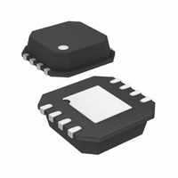
ADL5541ACPZ-R7 Analog Devices Inc, ADL5541ACPZ-R7 Datasheet

ADL5541ACPZ-R7
Specifications of ADL5541ACPZ-R7
ADL5541ACPZ-R7TR
Q3394642
Available stocks
Related parts for ADL5541ACPZ-R7
ADL5541ACPZ-R7 Summary of contents
Page 1
FEATURES Fixed gain Operation GHz Input/output internally matched to 50 Ω Integrated bias control circuit Output IP3 44 dBm at 500 MHz 40 dBm at 900 MHz Output 1 dB compression: 19.7 dBm at ...
Page 2
ADL5541 TABLE OF CONTENTS Features .............................................................................................. 1 Functional Block Diagram .............................................................. 1 General Description ......................................................................... 1 Revision History ............................................................................... 2 Specifications..................................................................................... 3 Typical Scattering Parameters..................................................... 5 Absolute Maximum Ratings............................................................ 6 ESD Caution.................................................................................. 6 Pin Configuration and Function Descriptions............................. 7 REVISION ...
Page 3
SPECIFICATIONS VPOS = 5 V and T = 25°C, unless otherwise noted. A Table 1. Parameter OVERALL FUNCTION Frequency Range Gain (S21) Input Return Loss (S11) Output Return Loss (S22) Reverse Isolation (S12) FREQUENCY = 100 MHz Gain Output 1 ...
Page 4
ADL5541 Parameter FREQUENCY = 3500 MHz Gain vs. Frequency vs. Temperature vs. Supply Output 1 dB Compression Point Output Third-Order Intercept Noise Figure FREQUENCY = 5800 MHz Gain vs. Frequency vs. Temperature vs. Supply Output 1 dB Compression Point Output ...
Page 5
TYPICAL SCATTERING PARAMETERS VPOS = 5 V and T = 25°C, the effects of the test fixture have been de-embedded up to the pins of the device. A Table 2. S11 Freq. (MHz) Magnitude (dB) Angle (°) 50 −18.11 −134.53 ...
Page 6
ADL5541 ABSOLUTE MAXIMUM RATINGS Table 3. Parameter Supply Voltage, VPOS Input Power (re: 50 Ω) Internal Power Dissipation (Paddle Soldered) θ (Junction to Paddle) JC Maximum Junction Temperature Operating Temperature Range Storage Temperature Range Stresses above those listed under Absolute ...
Page 7
PIN CONFIGURATION AND FUNCTION DESCRIPTIONS Table 4. Pin Function Descriptions Pin No. Mnemonic Description 1 RFIN RF Input. Requires a dc blocking capacitor GND Ground. Connect these pins to a low impedance ground plane ...
Page 8
ADL5541 TYPICAL PERFORMANCE CHARACTERISTICS 45 40 OIP3 (0dBm P1dB 15 GAIN 0.5 0.9 1.3 1.7 2.1 2.5 2.9 3.3 3.7 FREQUENCY (GHz) Figure 3. Gain, P1dB, OIP3, and Noise Figure vs. Frequency ...
Page 9
OIP3 (dBm) Figure 9. OIP3 Distribution at 900 MHz 19.4 19.5 19.6 19.7 19.8 19.9 20.0 P1dB (dBm) Figure 10. P1dB Distribution at ...
Page 10
ADL5541 BASIC CONNECTIONS The basic connections for operating the ADL5541 are shown in Figure 13. Recommended components are listed in Table 5. The input and output should be ac-coupled with appropriately sized capacitors (device characterization was performed with 33 pF ...
Page 11
EVALUATION BOARD Figure 19 shows the schematic for the ADL5541 evaluation board. The board is powered by a single 5 V supply. The components used on the board are listed in Table 6. Power can be applied to the board ...
Page 12
... OUTLINE DIMENSIONS PIN 1 INDICATOR 0.90 MAX 0.85 NOM SEATING PLANE ORDERING GUIDE Model Temperature Range 1 ADL5541ACPZ-R7 −40°C to +85°C 1 ADL5541-EVALZ RoHS Compliant Part. Visit www.analog.com/rfamps for the latest information on the Analog Devices, Inc., entire RF amplifier portfolio. Visit www.analog.com/rf for the latest information on the Analog Devices entire RF portfolio. ...


