WS2512-TR1 Avago Technologies US Inc., WS2512-TR1 Datasheet - Page 3
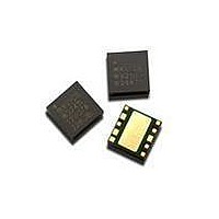
WS2512-TR1
Manufacturer Part Number
WS2512-TR1
Description
MODULE PA UMTS2100 4X4MM 10-PIN
Manufacturer
Avago Technologies US Inc.
Type
Power Amplifierr
Specifications of WS2512-TR1
Package / Case
10-DFN
Current - Supply
465mA ~ 510mA
Frequency
1.92GHz ~ 1.98GHz
Gain
23.5dB ~ 26.5dB
Rf Type
W-CDMA, HSPDA
Voltage - Supply
3.2V ~ 4.2V
Operating Frequency
1980 MHz
Operating Supply Voltage
4.2 V
Supply Current
510 mA
Maximum Operating Temperature
+ 90 C
Mounting Style
SMD/SMT
Minimum Operating Temperature
- 20 C
Number Of Channels
1 Channel
Frequency (max)
1.98GHz
Power Supply Requirement
Single
Single Supply Voltage (min)
3.2V
Single Supply Voltage (typ)
3.4V
Single Supply Voltage (max)
4.2V
Package Type
SMD
Dual Supply Voltage (min)
Not RequiredV
Dual Supply Voltage (typ)
Not RequiredV
Dual Supply Voltage (max)
Not RequiredV
Operating Temperature Classification
Commercial
Operating Temp Range
-20C to 90C
Pin Count
10
Mounting
Surface Mount
Lead Free Status / RoHS Status
Lead free / RoHS Compliant
Noise Figure
-
P1db
-
Test Frequency
-
Lead Free Status / Rohs Status
Compliant
Available stocks
Company
Part Number
Manufacturer
Quantity
Price

Part Number:
WS2512-TR1
Manufacturer:
AVAGO/安华高
Quantity:
20 000
Company:
Part Number:
WS2512-TR1G
Manufacturer:
AvagoTechnol
Quantity:
4 499


3
Table 4. Electrical Characteristics for WCDMA Mode (Vref=2.85V, Vcc=3.4V, Temp=+25°C)
Operating Frequency Range
Gain
ACLR in High power mode
ACLR in Mid power mode
ACLR in Low power mode
Harmonic Suppression
Input VSWR
Stability (Spurious Output)
Noise Power in Rx Band
Notes:
1. Electrical characteristics are specified under HSDPA modulated Up-Link signal (DPCCH/DPDCH=12/15, HS-DPCCH/DPDCH=15/15)
2. Specified under WCDMA modulated (3GPP Uplink DPCCH + 1DPDCH) signal.
3. Control current when series 6.2kohm is used.
4. ACP is expressed as a ratio of total adjacent power to signal power, both with 3.84 MHz bandwidth at specified offsets.
Characteristics
Power Added Efficiency
Total Supply Current
Quiescent Current
Reference Current
Control Current
Total Current in Power-down mode
ACLR in High power mode
unless specified otherwise.
[3]
[4]
[4]
[4]
[4]
5 MHz offset ACLR1_hiw
10 MHz offset ACLR2_hiw
5 MHz offset ACLR1_hi
10 MHz offset ACLR2_hi
5 MHz offset ACLR1_mid
10 MHz offset ACLR2_mid
5 MHz offset ACLR1_low
10 MHz offset ACLR2_low
Second
Third
Symbol
F
Gain_hiw
Gain_hi
Gain_mid
Gain_low
PAE_hiw
PAE_hi
PAE_mid
PAE_low
Icc_hiw
Icc_hi
Icc_mid
Icc_low
Iq_mid
Iq_low
Iref_hi
Iref_mid
Iref_low
Icont_mid
Icont_low
Ipd
2f0
3f0
VSWR
S
RxBN
Iq_hi
[2]
[2]
[2]
[2]
[2]
Condition
High Power Mode, Pout=28.0 dBm
High Power Mode, Pout=27.0 dBm
Mid Power Mode, Pout=16.0 dBm
Low Power Mode, Pout=7.0 dBm, Vcc=1.5V 10
High Power Mode, Pout=28.0 dBm
High Power Mode, Pout=27.0 dBm
Mid Power Mode, Pout=16.0 dBm
Low Power Mode, Pout=7.0 dBm, Vcc=1.5V 10.3
High Power Mode, Pout=28.0 dBm
High Power Mode, Pout=27.0 dBm
Mid Power Mode, Pout=16.0 dBm
Low Power Mode, Pout=7.0 dBm, Vcc=1.5V
High Power Mode
Mid Power Mode
Low Power Mode, Vcc=1.5V
High Power Mode
Mid Power Mode
Low Power Mode, Vcc=1.5V
Mid Power Mode
Low Power Mode, Vcc=1.5V
Vref=0.0V
High Power Mode, Pout=28.0 dBm
High Power Mode, Pout=28.0 dBm
High Power Mode, Pout=27.0 dBm
High Power Mode, Pout=27.0 dBm
Mid Power Mode, Pout=16.0 dBm
Mid Power Mode, Pout=16.0 dBm
Low Power Mode, Pout=7.0 dBm, Vcc=1.5V –
Low Power Mode, Pout=7.0 dBm, Vcc=1.5V –
High Power Mode, Pout=28.0 dBm
High Power Mode, Pout=28.0 dBm
VSWR 6:1, All phase
High Power Mode, Pout=28.0 dBm
[1]
Min.
1920
23.5
23.5
14.5
36
33
16.4
45
7
5
–
–
–
–
–
–
–
–
–
–
–
Typ.
–
26.5
26.5
17.5
13.0
40
37
21.5
14
465
400
54
22
65
13
11
3.5
4
4
0.18
0.18
0.2
-42
-55
-40
-54
-45
-57
-41
-54
-42
-64
2:1
–
-139
Max.
1980
510
445
70
33
90
22
18
7
8
8
1
1
5
-37
-47
-37
-47
-37
-47
-37
-47
-30
-45
2.5:1
-60
-136
Unit
MHz
dB
dB
dB
dB
%
%
%
%
mA
mA
mA
mA
mA
mA
mA
mA
mA
mA
mA
mA
µA
dBc
dBc
dBc
dBc
dBc
dBc
dBc
dBc
dBc
dBc
dBc
dBm/Hz
Related parts for WS2512-TR1
Image
Part Number
Description
Manufacturer
Datasheet
Request
R

Part Number:
Description:
MODULE PA UMTS2100 4X4MM 10-PIN
Manufacturer:
Avago Technologies US Inc.
Datasheet:

Part Number:
Description:
OPTOCOUPLER GATE DRV 2A 16-SOIC
Manufacturer:
Avago Technologies US Inc.
Datasheet:
Part Number:
Description:
OPTOCOUPLER 2CH 2.5A 16-SOIC
Manufacturer:
Avago Technologies US Inc.
Datasheet:

Part Number:
Description:
OPTOCOUPLER GATE DRV 0.4A 16SOIC
Manufacturer:
Avago Technologies US Inc.
Datasheet:

Part Number:
Description:
OPTOCOUPLER 2.0A 250KHZ 8-DIP
Manufacturer:
Avago Technologies US Inc.
Datasheet:

Part Number:
Description:
OPTOCOUPLER 2.0A 250KHZ GW 8-SMD
Manufacturer:
Avago Technologies US Inc.
Datasheet:

Part Number:
Description:
OPTOCOUPLER 2CH 15MBD 3.3V 8SOIC
Manufacturer:
Avago Technologies US Inc.
Datasheet:
Part Number:
Description:
OPTOCOUPLER DARL-OUT 8-DIP
Manufacturer:
Avago Technologies US Inc.
Datasheet:
Part Number:
Description:
OPTOCOUPLER IGBT DRIVE 0.4A 8DIP
Manufacturer:
Avago Technologies US Inc.
Datasheet:
Part Number:
Description:
OPTOCOUPLER DARL-OUT 8-DIP
Manufacturer:
Avago Technologies US Inc.
Datasheet:

Part Number:
Description:
OPTOCOUPLER 1CH 1MBS 8-SMD GW
Manufacturer:
Avago Technologies US Inc.
Datasheet:
Part Number:
Description:
OPTOCOUPLER GATE DRIVER 8-DIP
Manufacturer:
Avago Technologies US Inc.
Datasheet:

Part Number:
Description:
OPTOCOUPLER GATE DRIVER 8-SMD
Manufacturer:
Avago Technologies US Inc.
Datasheet:

Part Number:
Description:
OPTOCOUPLER PHOTOTRANS 4-SMD
Manufacturer:
Avago Technologies US Inc.
Datasheet:

Part Number:
Description:
OPTOCOUPLER W/BASE 6-DIP
Manufacturer:
Avago Technologies US Inc.
Datasheet: