ATAB5428-4-WB Atmel, ATAB5428-4-WB Datasheet - Page 55
ATAB5428-4-WB
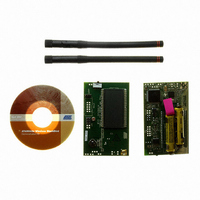
Manufacturer Part Number
ATAB5428-4-WB
Description
KIT DEMO 434MHZ BLACKBIRD
Manufacturer
Atmel
Series
Smart RFr
Type
Transceiver, UHFr
Specifications of ATAB5428-4-WB
Frequency
434MHz
Maximum Frequency
434 MHz
Output Power
0 dBm to 10 dBm
Supply Voltage (max)
6 V
Supply Voltage (min)
3 V
Supply Current
21 mA
Maximum Operating Temperature
+ 85 C
Board Size
2 in x 3.5 in
Minimum Operating Temperature
- 40 C
Product
RF Modules
For Use With/related Products
ATA5428
Lead Free Status / RoHS Status
Lead free / RoHS Compliant
Other names
ATAB-5428-4-WB


Figure 9-2.
4841D–WIRE–10/07
Sleep mode:
All circuits for analog signal processing are disabled. Only XTO and Polling logic is enabled.
Output level on pin RX_ACTIVE
T
Start-up mode:
Bit-check mode:
The incomming data stream is analyzed. If the timing indicates a valid transmitter signal,
the control bits VSOUT_EN, CLK_ON and OPM0 are set to 1 and the transceiver is set to
receiving mode. Otherwise the transceiver is set to Sleep mode
(if OPM0 = 0 and T
Output level on pin RX_ACTIVE
I
Receiving mode:
The incomming data stream is passed via PIN SDO_TMDO to the connected
microcontroller. If an bit error occurs the transceiver is not set back to Start-up mode.
Output level on pin RX_ACTIVE
I
S
S
Sleep
= I
= I
Start-up PLL:
The PLL is enabled and locked.
Output level on pin RX_ACTIVE
Start-up signal processing:
The signal processing circuit are enabled.
Output level on pin RX_ACTIVE
RX_X
RX_X
= Sleep
Start RX Mode
NO
; T
Flow Chart Polling Mode/RX Mode (T_MODE = 1, Transparent Mode Active)
Bit-check
1024
T
Sleep
OPM0 = 1
SLEEP
?
?
T
> 0) or stays in Bit-check mode.
DCLK
YES
YES
= 0
Start RX Polling Mode
X
Sleep
Low; I
High
High
RX data stream
available on pin
NO
High; I
High; I
SDO_TMDO
Level on pin
CS = Low ?
S
= I
NO
S
S
IDLE_X
= I
= I
YES
Startup_PLL_X
RX_X
Set VSOUT_EN = 1
Set CLK_ON = 1
; T
Set OPM0 = 1
Bit check
Startup_Sig_proc
OK ?
NO
; I
ATA5423/ATA5425/ATA5428/ATA5429
YES
Startup_PLL
Sleep:
X
T
T
T
T
DCLK
Startup_PLL
Startup_Sig_Proc
Bit-check
Sleep
:
:
:
:
:
Defined by bits Sleep 0 to Sleep 4 in Control
Register 4
Defined by bit XSleep in Control register 4
Basic clock cycle
798.5
882
498
306
210
Is defined by the selected baud rate range and
T
Baud 0 and Baud 1 in Control Register 6.
Depends on the result of the bit check.
If the bit check is ok, T
number of bits to be checked (N
on the utilized data rate.
If the bit check fails, the average time period for
that check despends on the selected bit-rate
range and on T
defined by bit Baud 0 and Baud 1 in Control
Register 6.
If in FSK mode the datastream is interrupted the
FSK-Demodulator-PLL tends to lock out and is
further not able to lock in, even there is a valid
data stream available.
In this case the transceiver must be set back to
IDLE mode.
DCLK
T
T
T
T
.The baud-rate range is defined by bit
DCLK
DCLK
DCLK
DCLK
T
DCLK
(typ)
XDCLK
(BR_Range 0)
(BR_Range 1)
(BR_Range 2)
(BR_Range 3)
. The bit-rate range is
Bit-check
depends on the
Bit-check
) and
55
Related parts for ATAB5428-4-WB
Image
Part Number
Description
Manufacturer
Datasheet
Request
R


Part Number:
Description:
KIT DEMO 868MHZ BLACKBIRD
Manufacturer:
Atmel
Datasheet:

Part Number:
Description:
BOARD BASESTATN UHF RCVR 433MHZ
Manufacturer:
Atmel
Datasheet:
Part Number:
Description:
BOARD BASESTATN UHF RCVR 868MHZ
Manufacturer:
Atmel
Datasheet:

Part Number:
Description:
DEV KIT FOR AVR/AVR32
Manufacturer:
Atmel
Datasheet:

Part Number:
Description:
INTERVAL AND WIPE/WASH WIPER CONTROL IC WITH DELAY
Manufacturer:
ATMEL Corporation
Datasheet:
Part Number:
Description:
Low-Voltage Voice-Switched IC for Hands-Free Operation
Manufacturer:
ATMEL Corporation
Datasheet:
Part Number:
Description:
MONOLITHIC INTEGRATED FEATUREPHONE CIRCUIT
Manufacturer:
ATMEL Corporation
Datasheet:
Part Number:
Description:
AM-FM Receiver IC U4255BM-M
Manufacturer:
ATMEL Corporation
Datasheet:
Part Number:
Description:
Monolithic Integrated Feature Phone Circuit
Manufacturer:
ATMEL Corporation
Datasheet:
Part Number:
Description:
Multistandard Video-IF and Quasi Parallel Sound Processing
Manufacturer:
ATMEL Corporation
Datasheet:
Part Number:
Description:
High-performance EE PLD
Manufacturer:
ATMEL Corporation
Datasheet: