SI1000DK Silicon Laboratories Inc, SI1000DK Datasheet - Page 12
SI1000DK
Manufacturer Part Number
SI1000DK
Description
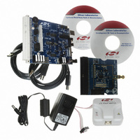
DEVELOPMENT KIT SI101X
Manufacturer
Silicon Laboratories Inc
Type
Development kitr
Specifications of SI1000DK
Mfg Application Notes
SI1000 Code Examples AppNote
Frequency
240MHz ~ 960MHz
Minimum Frequency
434 MHz
Supply Voltage (min)
7 V
Product
RF Development Tools
Maximum Frequency
915 MHz
Output Power
20 dBm
Antenna
SMA
Supply Voltage (max)
15 V
For Use With/related Products
Si100x
Lead Free Status / RoHS Status
Lead free / RoHS Compliant
Lead Free Status / RoHS Status
Lead free / RoHS Compliant, Lead free / RoHS Compliant
Other names
336-1880


Si10xx-DK
10. Motherboard
The Si1000 and Si1010 Development Kit includes a motherboard that enables evaluation and preliminary software
development. Numerous input/output (I/O) connections are provided to facilitate prototyping using the target board.
Refer to Figure 8 for the locations of the various I/O connectors. Figure 10 on page 14 shows the factory default
shorting block positions.
12
P1
P2
P3
J1
J2, J3, J4
J5
J6
J7
J8
J9
J10, J11
J12
J13
J14
J15
J16
J17
J18,J19
J20
H1
H2
SW4
SW5
Expansion connector (96-pin)
Power connector (accepts input from 7 to 15 VDC unregulated power adapter)
USB connector (connects to PC for serial communication)
Enable/Disable VBAT Power LED
Port I/O headers (provide access to Port I/O pins)
Enable/Disable VDD/DC+ Power LED
Provides an easily accessible ground clip
Connects pin P0.7 (IREF0 Output) to resistor R14 and capacitor C19
Connects P0.2 and P0.3 to switches and P1.5 and P1.6 to LEDs
DEBUG connector for Debug Adapter interface
Selects the power supply source (Wall Power, AAA Battery, or Coin Cell)
Connects Port I/O to UART0 interface
Connects external VREF capacitor to the P0.0/VREF
Connects the PCB ground plane to P0.1/AGND
Connects negative potentiometer (R14) terminal to pin P1.4 or to GND
Connects the potentiometer (R14) wiper to P0.6/CNVSTR
Creates an open in the power supply path to allow supply current measurement
Connects signals on P1 to the appropriate GPIO. Short J18 for Si100x and J19 for Si101x.
Connects signals on J18/J19 to the EEPROM accessible through P4.
Analog I/O terminal block
Provides terminal block access to the input and output nodes of J17
Switches the device between One-Cell (0.9–1.8 V supply) or Two-Cell (1.8–3.6 V) mode
Turns power to the MCU on or off
H1
R15
J18
J19
J20
J15
J16
Pin 1
P4
SILICON LABS
www.silabs.com
J5
VDD/DC+
Figure 8. Si1000 Motherboard
J3
J6
TOUCH SENSE SWITCH
J7
P0.6
`
Rev. 0.1
OFF
ON
J2
J13
J14
SW5
J4
J8
P1.6
P1.5
IMEASURE
AAA_BAT
RESET
COIN_CELL
WALL_PWR
J17
H2
USB POWER
P0.2
+1VD
+3VD
VBAT
J11
2103
J1
VBAT
U3
CP
P0.3
J12
P2
P3
SW4
J9
Pin 1
Pin 2
Related parts for SI1000DK
Image
Part Number
Description
Manufacturer
Datasheet
Request
R

Part Number:
Description:
QFN 42/I�/915 MHZ, SNAP ENABLED PROGRAMABLE XCVR
Manufacturer:
Silicon Laboratories Inc
Part Number:
Description:
QFN 42/I�/64KB, 4KB RAM, +20 DBM, PROGRAMMABLE XCVR
Manufacturer:
Silicon Laboratories Inc

Part Number:
Description:
IC TXRX MCU + EZRADIOPRO
Manufacturer:
Silicon Laboratories Inc
Datasheet:
Part Number:
Description:
Microcontrollers (MCU) 915MHz SNAP enabled program XCVR
Manufacturer:
Silicon Laboratories Inc
Datasheet:

Part Number:
Description:
BOARD EVALUATION FOR SI1000
Manufacturer:
Silicon Laboratories Inc
Datasheet:

Part Number:
Description:
BOARD EVALUATION FOR SI1000
Manufacturer:
Silicon Laboratories Inc
Datasheet:

Part Number:
Description:
BOARD EVALUATION FOR SI1012
Manufacturer:
Silicon Laboratories Inc
Datasheet:

Part Number:
Description:
BOARD EVALUATION FOR SI1002
Manufacturer:
Silicon Laboratories Inc
Datasheet:

Part Number:
Description:
DEVELOPMENT KIT SI101X
Manufacturer:
Silicon Laboratories Inc
Datasheet:

Part Number:
Description:
BOARD EVALUATION FOR SI1004
Manufacturer:
Silicon Laboratories Inc
Datasheet:

Part Number:
Description:
BOARD EVALUATION FOR SI1004
Manufacturer:
Silicon Laboratories Inc
Datasheet:
Part Number:
Description:
BOARD EVALUATION FOR SI1012
Manufacturer:
Silicon Laboratories Inc
Datasheet:
Part Number:
Description:
BOARD EVALUATION FOR SI1014
Manufacturer:
Silicon Laboratories Inc
Datasheet: