AD630BD Analog Devices Inc, AD630BD Datasheet - Page 3
AD630BD
Manufacturer Part Number
AD630BD
Description
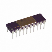
IC MOD/DEMOD BAL 2MHZ 20-CDIP
Manufacturer
Analog Devices Inc
Datasheet
1.AD630JNZ.pdf
(12 pages)
Specifications of AD630BD
Rohs Status
RoHS non-compliant
Function
Modulator/Demodulator
Frequency
2MHz
Package / Case
20-CDIP (0.300", 7.62mm)
Rf Type
Balanced
Supply Voltage Range
± 5V To ± 16V
Rf Ic Case Style
DIP
No. Of Pins
20
Operating Temperature Range
-25°C To +85°C
Peak Reflow Compatible (260 C)
No
Mounting Type
Through Hole
Supply Voltage Min
5V
Rohs Compliant
No
Digital Ic Case Style
DIP
Ic Function
Balanced Modulator/Demodulator
Lead Free Status / RoHS Status
Contains lead / RoHS non-compliant
Available stocks
Company
Part Number
Manufacturer
Quantity
Price


ABSOLUTE MAXIMUM RATINGS
Supply Voltage . . . . . . . . . . . . . . . . . . . . . . . . . . . . . . . . ± 18 V
Internal Power Dissipation . . . . . . . . . . . . . . . . . . . . 600 mW
Output Short-Circuit to Ground . . . . . . . . . . . . . . . Indefinite
Storage Temperature, Ceramic Package . . . –65°C to +150°C
Storage Temperature, Plastic Package . . . . . –55°C to +125°C
Lead Temperature Range (Soldering, 10 sec) . . . . . . . . 300°C
Maximum Junction Temperature . . . . . . . . . . . . . . . . . 150°C
REV. E
CHIP AVAILABILITY
The AD630 is available in laser trimmed, passivated chip
form. The figure above shows the AD630 metallization pattern,
bonding pads and dimensions. AD630 chips are available; con-
sult factory for details.
CAUTION
ESD (electrostatic discharge) sensitive device. Electrostatic charges as high as 4000 V readily
accumulate on the human body and test equipment and can discharge without detection. Although
the AD630 features proprietary ESD protection circuitry, permanent damage may occur on devices
subjected to high energy electrostatic discharges. Therefore, proper ESD precautions are
recommended to avoid performance degradation or loss of functionality.
CHIP METALLIZATION AND PINOUT
Model
AD630JN
AD630KN
AD630AR
AD630AR-REEL
AD630AD
AD630BD
AD630SD
AD630SD/883B
5962-8980701RA
AD630SE/883B
5962-89807012A
AD630JCHIPS
AD630SCHIPS
Dimensions shown in inches and (millimeters).
Contact factory for latest dimensions.
Temperature Ranges
0°C to 70°C
0°C to 70°C
–25°C to +85°C
–25°C to +85°C
–25°C to +85°C
–25°C to +85°C
–55°C to +125°C
–55°C to +125°C
–55°C to +125°C
–55°C to +125°C
–55°C to +125°C
0°C to 70°C
–55°C to +125°C
ORDERING GUIDE
Package Description
PDIP
PDIP
SOIC
SOIC 13" Tape and Reel
SBDIP
SBDIP
SBDIP
SBDIP
SBDIP
CLCC
CLCC
Chip
Chip
–3–
20-Lead PDIP (N)
20-Lead Ceramic DIP (D)
20-Lead Leadless Chip Carrier LCC (E)
20-Lead SOIC (R-20)
CHANNEL STATUS B/A
CHANNEL STATUS B/A
DIFF OFF ADJ
CM OFF ADJ
CM OFF ADJ
20-Lead SOIC, PDIP, and CERDIP
DIFF OFF ADJ
DIFF OFF ADJ
THERMAL CHARACTERISTICS
CM OFF ADJ
CM OFF ADJ
–V
PIN CONFIGURATIONS
CH A+
SEL B
SEL A
S
R
–V
4
5
6
7
8
IN
Package Option
N-20
N-20
R-20
D-20
D-20
D-20
D-20
D-20
E-20A
E-20A
20-Terminal CLCC
R-20
A
S
10
8
9
1
2
3
4
5
6
7
3
9 10 11 12 13
(Not to Scale)
(Not to Scale)
TOP VIEW
TOP VIEW
2
AD630
AD630
1
20 19
20
19
18
17
16
15
14
13
12
11
CH A–
CH B–
CH B+
R
R
R
R
V
COMP
+V
OUT
IN
A
F
B
18
17
16
15
14
S
B
24°C/W
35°C/W
35°C/W
38°C/W
CH B+
R
R
R
R
JC
IN
A
F
B
B
AD630
61°C/W
120°C/W
120°C/W
75°C/W
JA
Related parts for AD630BD
Image
Part Number
Description
Manufacturer
Datasheet
Request
R

Part Number:
Description:
±1.7g Dual-Axis IMEMS Accelerometer Evaluation Board
Manufacturer:
Analog Devices Inc
Datasheet:

Part Number:
Description:
Inertial Sensor Evaluation System
Manufacturer:
Analog Devices Inc
Datasheet:
Part Number:
Description:
Manufacturer:
Analog Devices Inc
Datasheet:
Part Number:
Description:
Manufacturer:
Analog Devices Inc
Datasheet:
Part Number:
Description:
Manufacturer:
Analog Devices Inc
Datasheet:
Part Number:
Description:
Manufacturer:
Analog Devices Inc
Datasheet:
Part Number:
Description:
Manufacturer:
Analog Devices Inc
Datasheet:
Part Number:
Description:
Manufacturer:
Analog Devices Inc
Datasheet:
Part Number:
Description:
Manufacturer:
Analog Devices Inc
Datasheet:
Part Number:
Description:
Manufacturer:
Analog Devices Inc
Datasheet:
Part Number:
Description:
Manufacturer:
Analog Devices Inc
Datasheet:
Part Number:
Description:
Manufacturer:
Analog Devices Inc
Datasheet:
Part Number:
Description:
Manufacturer:
Analog Devices Inc
Datasheet: