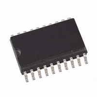
T5744N-TKQ Atmel, T5744N-TKQ Datasheet

T5744N-TKQ
Specifications of T5744N-TKQ
Related parts for T5744N-TKQ
T5744N-TKQ Summary of contents
Page 1
Features • Minimal External Circuitry Requirements Components on the PC Board Except Matching to the Receiver Antenna • High Sensitivity, Especially at Low Data Rates • SSO20 and SO20 package • Fully Integrated VCO • Supply Voltage 4.5 ...
Page 2
Pin Configuration Figure 2. Pinning SO20 and SSO20 Pin Description Pin Symbol 1 BR_0 2 BR_1 3 CDEM 4 AVCC 5 AGND 6 DGND 7 MIXVCC 8 LNAGND 9 LNA_IN 10 n.c. 11 LFVCC LFGND 14 XTO ...
Page 3
Figure 3. Block Diagram CDEM RSSI AVCC AGND DGND MIXVCC LNAGND LNA_IN RF Front End 4521B–RKE–01/03 BR_0 BR_1 ASK- Dem_out Demodulator and data filter RSSI RSSI IF Amp 4. Order LPF 3 MHz IF Amp VCO LPF 3 MHz f ...
Page 4
T5744 4 Figure 4. PLL Peripherals DVCC XTO LFGND LF LFVCC The passive loop filter connected to Pin LF is designed for a loop bandwidth of BLoop = 100 kHz. This value for BLoop exhibits the best possible noise performance ...
Page 5
Table 1. Calculation of LO and IF Frequency Conditions f = 315 MHz, MODE = 433.92 MHz, MODE = 1 RF 300 MHz < f < 365 MHz, MODE = 0 RF 365 MHz < f ...
Page 6
Figure 6. Input Matching Network without SAW Filter f = 433.92 MHz RF C3 25n 15p RF IN 3.3p 100p 22n TOKO LL2012 F22NJ Analog Signal Processing IF Amplifier RSSI Amplifier Pin RSSI T5744 LNAGND T5744 ...
Page 7
ASK Demodulator and Data Filter 4521B–RKE–01/03 Figure 7. RSSI Characteristics 3.0 2.8 2.6 2.4 25°C 2.2 105°C 2.0 1.8 1.6 1.4 1.2 1.0 -130.0 -110.0 The signal coming from the RSSI amplifier is converted into the raw data signal by ...
Page 8
Receiving Characteristics Basic Clock Cycle of the Digital Circuitry T5744 8 The RF receiver T5744 can be operated with and without a SAW front-end filter typical automotive application, a SAW filter is used to achieve better selectivity. The ...
Page 9
Pin ENABLE 4521B–RKE–01/03 Pin MODE can now be set in accordance with the desired clock cycle T the following application-relevant parameters: Timing of the analog and digital signal processing IF filter center frequency (f ) IF0 Most applications are dominated ...
Page 10
Figure 10. Enable Timing (1) Dem_out ENABLE DATA Sleep mode Figure 11. Enable Timing (2) Dem_out ENABLE DATA Sleep mode Digital Signal Processing T5744 10 Start-up mode Soff ...
Page 11
Figure 12. Synchronization of the Demodulator Output T XClk Dem_out Data_out (DATA) Figure 13. Debouncing of the Demodulator Output Dem_out DATA t DATA_min Absolute Maximum Ratings Parameters Supply voltage Power dissipation Juntion temperature Storage temperature Ambient temperature Maximum input level, ...
Page 12
Electrical Characteristics All parameters refer to GND, T amb wise specified 25°C) S amb Test Conditions Parameters Basic Clock Cycle of the Digital Circuitry Basic clock MODE = 0 (USA) cycle MODE = 1 ...
Page 13
Electrical Characteristics (continued) Parameters Test Conditions Maximum input level Input matched according to Figure 6, BER £ 10 Local Oscillator Operating frequency range VCO Phase noise VCO / LO f osc at 1 MHz at 10 MHz Spurious of the ...
Page 14
Electrical Characteristics (continued) Parameters Test Conditions Dynamic range RSSI amplifier RSSI output voltage range RSSI gain RI of Pin CDEM for cut-off fcu_DF frequency calculation Recommended CDEM for BR_Range0 best performance BR_Range1 BR_Range2 BR_Range3 Upper cut-off frequency data Upper cut-off ...
Page 15
Figure 14. Application Circuit 2.2uF 10nF 10% 10% GND KOAX C17 3.3pF 5% np0 Figure 15. Application Circuit 2.2uF 10nF 10% 10% GND KOAX C17 3.3pF 5% np0 4521B–RKE–01/03 = ...
Page 16
Figure 16. Application Circuit 2.2uF 10nF 10% 10% GND L2 TOKO LL2012 KOAX F33NJ 1 2 33nH 8.2pF 5% np0 Figure 17. Application Circuit 2.2uF 10nF ...
Page 17
Ordering Information Extended Type Number T5744-TKS T5744-TKQ T5744-TGS T5744-TGQ Package Information Package SO20 Dimensions in mm 0.4 1. 4521B–RKE–01/03 Package Remarks SSO20 Tube SSO20 Taped and reeled SO20 Tube SO20 Taped and reeled 12.95 12.70 2.35 0.25 0.10 ...
Page 18
Package SSO20 Dimensions in mm 0.25 0. T5744 18 6.75 6.50 1.30 0.15 0.05 5.85 11 technical drawings according to DIN specifications 10 5.7 5.3 4.5 4.3 0.15 6.6 6.3 4521B–RKE–01/03 ...
Page 19
... No licenses to patents or other intellectual property of Atmel are granted by the Company in connection with the sale of Atmel products, expressly or by implication. Atmel’s products are not authorized for use as critical components in life support devices or systems. ...


