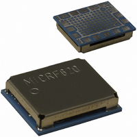
MICRF620Z Micrel Inc, MICRF620Z Datasheet
MICRF620Z
Specifications of MICRF620Z
MICRF620Z


Related parts for MICRF620Z

MICRF620Z Summary of contents
Page 1
... All support documentation can be found on Micrel’s web site at: www.micrel.com. RadioWire® trademark of Micrel, Inc. Micrel Inc. • 2180 Fortune Drive • San Jose, CA 95131 • USA • tel +1 ( July 2006 434MHz ISM Band Transceiver Module multi-channeled ...
Page 2
... Bit Synchronizer................................................................................................................................................................ 17 Transmitter ............................................................................................................................................................................ 17 Power Amplifier................................................................................................................................................................. 17 Frequency Modulation ...................................................................................................................................................... 17 Using the XCO-tune Bits ....................................................................................................................................................... 17 Application Circuit Illustration ................................................................................................................................................ 18 Assembling the MICRF620 ................................................................................................................................................... 19 Recommended Reflow Temperature Profile .................................................................................................................... 19 Shock/Vibration during Reflow.......................................................................................................................................... 19 Handassembling the MICRF620....................................................................................................................................... 19 Layout.................................................................................................................................................................................... 19 Recommended Land Pattern............................................................................................................................................ 19 Layout Considerations ...................................................................................................................................................... 20 Package Dimensions ............................................................................................................................................................ 21 Tape Dimensions .................................................................................................................................................................. 21 July 2006 2 MICRF620/MICRF620Z M9999-120205 ...
Page 3
... MHz MICRF610Z MICRF620 430-440 MHz MICRF620Z RFB433B 430-440 MHz RFB868B 868-870 MHz RFB915B 902-928 MHz Ordering Information Part Number MICRF620 TR MICRF620Z TR Block Diagram ANT July 2006 Supply Data Rate Receive Voltage <20 kbps 13.5 mA 2.0-2.5 v Lead-free MICRF600 <15 kbps 13 ...
Page 4
... Chip select, three wire programming interface I Clock, three wire programming interface I/O Data, three wire programming interface I/O Data receive/transmit, bi-directional O Data clock receive/transmit O Lock detect O Receive signal strength indicator Ground Ground Ground I/O RF In/Out Ground VDD (2.0-2.5V) Ground 4 MICRF620/MICRF620Z M9999-120205 ...
Page 5
... PA2_0: 111 LOAD R = 50Ω, PA2_0: 001 LOAD R = 50Ω, PA2_0: 111 LOAD Limited by receiver BW NRZ 19.2kbps, β (±85kHz), -36dBm (RBW=10kHz) ETSI EN300 220 5 MICRF620/MICRF620Z (2) ) ..................................+2.0V to +2. .......................–20°C to +75°C A < +75°C, unless noted. A Min Typ Max 2.0 2.5 0.3 ...
Page 6
... Offset ±1MHz Desired signal: Offset ±2MHz 19.2 kbps, β =6, Offset ±5MHz 3dB above sens, Offset ±10MHz SC=133 kHz Offset ±30MHz 2 tones with 1MHz separation ETSI 300-220 Pin = -100 dBm Pin = -60 dBm 6 MICRF620/MICRF620Z Min Typ Max 12 10.3 9.6 3 -110 -109 -108 -107 -105 +10 ...
Page 7
... M1_11 M1_5 M1_4 M1_3 ‘1’ ‘1’ ‘0’ FEEC_3 FEE_5 FEE_4 FEE_3 Table 1. Control Registers in MICRF620 7 MICRF620/MICRF620Z D2 D1 Mode1 Mode0 LD_en PF_FC1 PF_FC0 ‘0’ ‘0’ VCO_IB0 VCO_freq1 VCO_freq0 ‘0’ ‘0’ ‘0’ ‘0’ ...
Page 8
... ControlRegister21. Refer to the specific sections of this document for actual values. Table 4. “Address” and “R/W bit” together make 1 octet. In total, 23 octets are clocked into the MICRF620. 8 MICRF620/MICRF620Z Data to write into register i Internal load pulse made here ...
Page 9
... Data to write Data to write into register i into register i+1 Internal load pulse made here 9 MICRF620/MICRF620Z 1. Enter address and R/W bit 2. Change direction of IO line 3. Read out a number of octets and change IO direction back again. CS SCLK ...
Page 10
... Min. delay from rising edge of SCLK to valid IO during a read operation (assuming load capacitance 25pF) Table 6. Timing Specification for the 3-wire Programming Interface July 2006 traise Tper Thigh tfall Tlow Address Register Figure 4. Programming Interface Timing 10 MICRF620/MICRF620Z Tread Twrite Tscl Data Register LOAD Values Min. Typ ...
Page 11
... CS low for loading, i.e., activation of the new control register values. • Reading: Bring CS high, write address and R/W bit, set input, read present contents of the addressed control register(s), bring CS low and set IO an output. 11 MICRF620/MICRF620Z M9999-120205 ...
Page 12
... The bias bit will optimize the phase noise, and the frequency bit will control a capacitor bank in the VCO. The tuning range the RF frequency versus varactor voltage is dependent on the VCO frequency setting, and can be shown in Figure 6. When XCOtune4 – 12 MICRF620/MICRF620Z 55.0 45.0 35.0 25.0 15.0 5.0 -5 ...
Page 13
... Mode1 Mode0 State Comments 0 0 Power down Keeps register configuration 0 1 Standby Only crystal oscillator running 1 0 Receive Full receive 1 1 Transmit Full transmit ex PA state July 2006 1,6 2 2,4 = 2.5V LD_en PF_FC1 PF_FC0 Sync_en Mode1 Mode0 ’1’ 13 MICRF620/MICRF620Z M9999-120205 ...
Page 14
... If the I channel leads the Q channel, the FSK tone lies below the LO frequency (data ‘0’). The output of the receiver is available on the DataIXO pin. A RSSI circuit (receive signal strength indicator) indicates the received signal level. 14 MICRF620/MICRF620Z Sync_en Mode1 ...
Page 15
... A formula for the receiver bandwidth can be summarized as follows LD_en PF_FC1 PF_FC0 In battery operated applications that do not need very high selectivity, the main channel filter can be bypassed by SC_by=1. This will reduce the Rx current consumption with ~2mA. Cut-off Freq. (kHz) 15 MICRF620/MICRF620Z ‘ ...
Page 16
... To compensate for this, the receivers XCO frequency should be increased recommended to use Mode UP+DN for two reasons, you do not need to know the actual frequency deviation and this mode gives the best accuracy. 16 MICRF620/MICRF620Z FEEC_1 FEEC_0 FEE Mode 0 0 Off ...
Page 17
... Example: In FEE, count up+down pulses, counting 8 bits: A perfect case ==> FEE = 0 If FEE > too low, increase LO by decreasing XCO_tune value v.v. for FEE < 0 FEE field holds a number in the range -128, … , 127. However, it keeps counting above/below the range, which is: 17 MICRF620/MICRF620Z RefClk_K2 RefClk_K1 between the two ...
Page 18
... Figure 11 shows a recommended voltage divider circuit for a MCU running at 3.0V and the MICRF620 at 2.5V. July 2006 MICRF6xx CS SCLK IO DATAIXO DATACLK LD RSSI Figure 12. How to connect MICRF620 (2.5V) and MCU (3.0V) and a mikro- 18 MICRF620/MICRF620Z MCU 3k3 CS 18k 3k3 SCLK 18k 3k3 IO 18k 15k DATAIXO DATACLK ...
Page 19
... July 2006 Layout Recommended Land Pattern Figure 14 shows a recommended land pattern that facilitates both automatic and hand assembling. Figure 14. Recommended Land Pattern (TOP VIEW) 19 MICRF620/MICRF620Z M9999-120205 ...
Page 20
... Digital high speed should/must safe distance from RF circuitry or RF VDD as this might/will cause degradation of sensitivity and create spurious emissions. Example of such circuitry is LCD display, charge pumps, RS232, clock / data bus etc. 20 MICRF620/MICRF620Z logic or noisy circuitry M9999-120205 ...
Page 21
... Purchaser’s use or sale of Micrel Products for use in life support appliances, devices or systems is a Purchaser’s own risk and Purchaser agrees to fully July 2006 Figure 15. Package Dimensions Figure 16. Tape Dimensions indemnify Micrel for any damages resulting from such use or sale. © 2005 Micrel, Incorporated. 21 MICRF620/MICRF620Z nt M9999-120205 ...