DP1205C433LF Semtech, DP1205C433LF Datasheet - Page 3
DP1205C433LF
Manufacturer Part Number
DP1205C433LF
Description
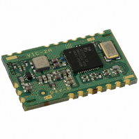
MODULE DROP IN FOR XE1205 433MHZ
Manufacturer
Semtech
Datasheet
1.DP1205C433.pdf
(13 pages)
Specifications of DP1205C433LF
Frequency
433MHz
Data Rate - Maximum
153.2kbps
Applications
ISM
Power - Output
11dBm
Sensitivity
-111dBm
Voltage - Supply
2.4 V ~ 3.6 V
Current - Receiving
14mA
Current - Transmitting
62mA
Data Interface
PCB, Surface Mount
Antenna Connector
PCB, Surface Mount
Operating Temperature
-40°C ~ 85°C
Package / Case
Module
Operating Temperature (min)
-40C
Operating Temperature (max)
85C
Operating Temperature Classification
Industrial
Operating Supply Voltage (typ)
2.5/3.3V
Operating Supply Voltage (max)
3.6V
Lead Free Status / RoHS Status
Lead free / RoHS Compliant
Memory Size
-
Modulation Or Protocol
-
Lead Free Status / Rohs Status
Compliant
Other names
DP1205C433LFTR
Available stocks
Company
Part Number
Manufacturer
Quantity
Price
Company:

Part Number:
DP1205C433LF
Manufacturer:
MOLEX
Quantity:
5 000


1
Please note that the leaded version of this product exhibits a non-conformance. The non-conformance affects the
CLKOUT signal of the DP1205 which is not enabled at power-up of the module. It is also recommended to program all
registers after power-up of the module. The Lead-Free version (suffix "LF") of this product does not exhibit these non-
conformances.
Please note that all products whose date-codes are before 0706 (wwyy) exhibit a non-conformance to specification. The
non-conformance affects the FIFO buffer of the XE1205 transceiver contained in this module as described in section 5 -
Data operation modes. For these date-codes, please use the FIFO in this product only in conjunction with the Technical
Note TN1205.01 (available from the SEMTECH web site). All other date-codes are in conformance with the specification.
2
PIN
1
2
3
4
5
6
7
8
9
10
11
12
13
14
15
16
17
18
19
© Semtech 2006
NON-CONFORMANCE
PIN DESCRIPTION
NSS_CONFIG
RF_IN_OUT
NSS_DATA
CLKOUT
NAME
VDDA
SW(0)
SW(1)
DATA
MISO
MOSI
IRQ0
IRQ1
GND
GND
GND
GND
GND
VDD
SCK
IN/OUT
IN/OUT
IN/OUT
IN/OUT
OUT
OUT
OUT
OUT
I/O
IN
IN
IN
IN
DESCRIPTION
Ground
RF Input / Output terminal
Ground
Supply Voltage
Ground
Supply Voltage
SPI SELECT CONFIG
SPI SELECT DATA / DATAIN
Interrupt (PATTERN/FIFOEMPTY)
Ground
Ground
Interrupt (DCLK/FIFOFULL)
Data
Output clock at reference frequency divided by 2, 4, 8, 16, 32
SPI Master Input Slave Output
SPI Master Output Slave Input
SPI CLOCK
Transmit/Receive/Stand-by/Sleep Mode Select
Transmit/Receive/Stand-by/Sleep Mode Select
1
2
3
19
18
3
17
4
16
5
15
6
14
7
13
8
12
9 10
11
433/868/915 MHz RF Modules
www.semtech.com
DP1205
Related parts for DP1205C433LF
Image
Part Number
Description
Manufacturer
Datasheet
Request
R

Part Number:
Description:
Test Probes DIFFERENTIAL PROBE
Manufacturer:
Fluke
Datasheet:

Part Number:
Description:
EVALUATION BOARD
Manufacturer:
Semtech
Datasheet:
Part Number:
Description:
EVALUATION BOARD
Manufacturer:
Semtech
Datasheet:
Part Number:
Description:
VOLTAGE SUPPRESSOR, TRANSIENT SEMTECH
Manufacturer:
Semtech
Datasheet:

Part Number:
Description:
HIGH VOLTAGE CAPACITORS MONOLITHIC CERAMIC TYPE
Manufacturer:
Semtech Corporation
Datasheet:
Part Number:
Description:
EZ1084CM5.0 AMP POSITIVE VOLTAGE REGULATOR
Manufacturer:
Semtech Corporation
Datasheet:
Part Number:
Description:
3.0 AMP LOW DROPOUT POSITIVE VOLTAGE REGULATORS
Manufacturer:
Semtech Corporation
Datasheet:
Part Number:
Description:
Manufacturer:
Semtech Corporation
Datasheet:
Part Number:
Description:
RailClamp Low Capacitance TVS Diode Array
Manufacturer:
Semtech Corporation
Datasheet:
Part Number:
Description:
Manufacturer:
Semtech Corporation
Datasheet:
Part Number:
Description:
Manufacturer:
Semtech Corporation
Datasheet:
Part Number:
Description:
Manufacturer:
Semtech Corporation
Datasheet: