CM100RX-12A Powerex Inc, CM100RX-12A Datasheet - Page 4
CM100RX-12A
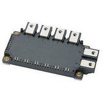
Manufacturer Part Number
CM100RX-12A
Description
IGBT MOD 7PAC 600V 100A NX SER
Manufacturer
Powerex Inc
Series
IGBTMOD™r
Type
IGBTr
Datasheet
1.CM100RX-12A.pdf
(6 pages)
Specifications of CM100RX-12A
Configuration
Three Phase Inverter with Brake
Voltage - Collector Emitter Breakdown (max)
600V
Vce(on) (max) @ Vge, Ic
2.1V @ 15V, 100A
Current - Collector (ic) (max)
100A
Current - Collector Cutoff (max)
1mA
Input Capacitance (cies) @ Vce
13.3nF @ 10V
Power - Max
400W
Input
Standard
Ntc Thermistor
Yes
Mounting Type
Chassis Mount
Package / Case
Module
Dc Collector Current
100A
Collector Emitter Voltage Vces
600V
Power Dissipation Pd
10mW
Collector Emitter Voltage V(br)ceo
600V
Operating Temperature Range
-40°C To +150°C
No. Of Pins
23
Voltage
600V
Current
100A
Circuit Configuration
7-PAC
Rohs Compliant
Yes
Recommended Gate Driver
M57959L
Recommended Dc To Dc Converter
VLA106-15242
Lead Free Status / RoHS Status
Lead free / RoHS Compliant
For Use With
BG2B-5015 - KIT DEV BOARD 2CN 5A FOR IGBTBG2B-3015 - KIT DEV BOARD 2CN 3A FOR IGBTBG2B-1515 - KIT DEV BOARD 1.5A FOR IGBTBG2A-NF - KIT DEV BOARD FOR IGBT
Igbt Type
-
Lead Free Status / RoHS Status
Lead free / RoHS Compliant, Lead free / RoHS Compliant


4
Powerex, Inc., 173 Pavilion Lane, Youngwood, Pennsylvania 15697 (724) 925-7272
CM100RX-12A
Six IGBTMOD™ + Brake NX-Series Module
100 Amperes/600 Volts
Electrical and Mechanical Characteristics, T
Brake Sector
Characteristics
Collector Cutoff Current
Gate-Emitter Threshold Voltage
Gate Leakage Current
Collector-Emitter Saturation Voltage
Input Capacitance
Output Capacitance
Reverse Transfer Capacitance
Total Gate Charge
Repetitive Reverse Current
Forward Voltage Drop
Thermal and Mechanical Characteristics, T
Characteristics
Thermal Resistance, Junction to Case**
Thermal Resistance, Junction to Case**
Contact Thermal Resistance**
Internal Gate Resistance
External Gate Resistance
NTC Thermistor Sector, T
Characteristics
Zero Power Resistance
Deviation of Resistance
B Constant
Power Dissipation
**Thermal resistance values are per 1 element.
*1 Case temperature (T
*2 I
*5 Pulse width and repetition rate should be such as to cause negligible temperature rise.
*7 Typical value is measured by using thermally conductive grease of λ = 0.9 [W/(m • K)].
I
E
F
, I
, I
FM
EM
, I
, V
RRM
EC
, t
, V
rr
FM
and Q
and V
C
) and heatsink temperature (T
rr
represent ratings and characteristics of the anti-parallel, emitter-to-collector free-wheel diode (FWDi).
RRM
represent ratings and characteristics of the clamp diode.
j
= 25°C unless otherwise specified
R
V
R
B
V
Symbol
I
Symbol
Symbol
V
R
CE(sat)
RRM
R
f
th(j-c)
th(j-c)
∆R/R
I
I
C
(25/50)
GE(th)
C
) are defined on the surface of the baseplate and heatsink at just under the chip.
C
GES
P
CES
Q
FM
th(j-f)
R
Gint
oes
R
res
ies
25
G
G
*2
*2
Q
D
j
j
= 25°C unless otherwise specified
= 25°C unless otherwise specified
B = (InR
V
Case to Heatsink (Per 1 Module)
CC
I
C
I
Thermal Grease Applied
T
C
C
= 50A, V
= 300V, I
= 50A, V
I
V
C
= 100°C, R
V
V
CE
I
1
= 50A, V
I
F
CE
GE
F
I
Test Conditions
Test Conditions
– InR
F
= 50A, T
T
T
Test Conditions
= 10V, V
V
= 50A, T
Per FWDi
Per IGBT
T
= V
= 50A, Chip
C
C
= V
R
C
GE
C
GE
I
= 25°C
= 25°C
= V
C
= 25°C
CES
GES
2
= 50A, V
) / (1/T
= 5mA
= 15V, T
GE
100
= 15V, T
RRM
j
GE
, V
j
, V
= 125°C
= 15V, Chip
= 25°C
*1
*1
*1
*1
= 493Ω
GE
CE
= 0V
1
GE
j
– 1/T
= 0V
= 0V
j
= 125°C
= 25°C
*5
*1*7
= 15V
*5
*1
2
)
*6
*5
*5
Min.
Min.
Min.
4.85
–7.3
13
—
—
—
—
—
—
—
—
—
—
—
—
—
—
—
—
—
—
—
5
0.015
3375
5.00
1.95
Typ.
Typ.
200
Typ.
2.0
1.7
1.9
1.6
1.9
—
—
—
—
—
—
—
—
—
—
—
6
0
Max.
Max.
Max.
0.44
0.85
5.15
+7.8
125
1.0
0.5
2.1
9.3
0.3
1.0
2.8
1.0
—
—
—
—
—
—
—
—
10
7
°C/W
°C/W
°C/W
Units
Volts
Volts
Volts
Volts
Volts
Volts
Volts
Units
Units
Rev. 3/09
mW
mA
mA
nC
µA
nF
nF
nF
kΩ
%
Ω
Ω
K
Related parts for CM100RX-12A
Image
Part Number
Description
Manufacturer
Datasheet
Request
R

Part Number:
Description:
IGBT MOD 7PAC 1200V 100A NX SER
Manufacturer:
Powerex Inc
Datasheet:

Part Number:
Description:
IGBT MODULE NX-SERIES 7-PAC DP 1200 100
Manufacturer:
Powerex Inc
Datasheet:


Part Number:
Description:
RF Devices / Rectifier Diodes
Manufacturer:
Bharat Electronics Ltd
Part Number:
Description:
Molded Mini-dyad
Manufacturer:
ETC-unknow
Datasheet:
Part Number:
Description:
Plug Connector
Manufacturer:
DDK Ltd.
Datasheet:
Part Number:
Description:
Molded Mini-DYAD
Manufacturer:
CLARE [Clare, Inc.]
Datasheet:
Part Number:
Description:
One-Touch Locking Style Small Sized Circular Connectors
Manufacturer:
DDK [DDK Ltd.]
Datasheet:

Part Number:
Description:
INDUCTOR CHIP SMD
Manufacturer:
Bourns Inc.
Datasheet:
Part Number:
Description:
INDUCTOR CHIP SMD
Manufacturer:
Bourns Inc.
Datasheet:
Part Number:
Description:
INDUCTOR CHIP SMD
Manufacturer:
Bourns Inc.
Datasheet:
Part Number:
Description:
INDUCTOR CHIP SMD
Manufacturer:
Bourns Inc.
Datasheet:
Part Number:
Description:
INDUCTOR CHIP SMD
Manufacturer:
Bourns Inc.
Datasheet:
Part Number:
Description:
INDUCTOR CHIP SMD
Manufacturer:
Bourns Inc.
Datasheet: