T70RIA60 Vishay, T70RIA60 Datasheet - Page 2
T70RIA60
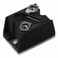
Manufacturer Part Number
T70RIA60
Description
SCR PHASE CONT 600V 70A D-55
Manufacturer
Vishay
Type
SCRr
Datasheet
1.T50RIA20.pdf
(12 pages)
Specifications of T70RIA60
Structure
Single
Number Of Scrs, Diodes
1 SCR
Voltage - Off State
600V
Current - Gate Trigger (igt) (max)
120mA
Current - On State (it (av)) (max)
70A
Current - On State (it (rms)) (max)
110A
Current - Non Rep. Surge 50, 60hz (itsm)
1660A, 1740A
Current - Hold (ih) (max)
200mA
Mounting Type
Chassis Mount
Package / Case
D-55 T-Module
Mounting Style
Through Hole
Repetitive Peak Off-state Volt
600V
Off-state Voltage
600V
Average On-state Current
70A
Hold Current
200mA
Gate Trigger Current (max)
120mA
Gate Trigger Voltage (max)
2.5V
Peak Reverse Gate Voltage
10V
Package Type
D-55
Peak Repeat Off Current
100uA
Peak Surge On-state Current (max)
1740A
On State Voltage(max)
1.55V
Mounting
Screw
Pin Count
3
Operating Temp Range
-40C to 125C
Operating Temperature Classification
Automotive
Lead Free Status / RoHS Status
Lead free / RoHS Compliant
Lead Free Status / RoHS Status
Lead free / RoHS Compliant, Lead free / RoHS Compliant
Other names
*T70RIA60
VS-T70RIA60
VS-T70RIA60
VST70RIA60
VST70RIA60
VS-T70RIA60
VS-T70RIA60
VST70RIA60
VST70RIA60


T..RIA Series
Vishay High Power Products
www.vishay.com
2
ON-STATE CONDUCTION
PARAMETER
Maximum average on-state current
at case temperature
Maximum RMS on-state current
Maximum peak, one-cycle
on-state, non-repetitive
surge current
Maximum I
Maximum I
Low level value of
threshold voltage
High level value of
threshold voltage
Low level value of
on-state slope resistance
High level value of
on-state slope resistance
Maximum on-state voltage drop
Maximum forward voltage drop
Maximum holding current
Maximum latching current
SWITCHING
PARAMETER
Typical turn-on time
Typical reverse recovery time
Typical turn-off time
2
2
t for fusing
√t for fusing
SYMBOL
SYMBOL
V
V
I
T(RMS)
I
I
T(TO)1
T(TO)2
V
V
T(AV)
TSM
t
I
For technical questions, contact: ind-modules@vishay.com
I
r
r
t
I
I
t
gd
2
2
TM
FM
t1
t2
H
rr
L
q
t
√t
T
I
T
T
-dI/dt = 15 A/µs, V
180° conduction, half sine wave
t = 10 ms
t = 8.3 ms
t = 10 ms
t = 8.3 ms
t = 10 ms
t = 8.3 ms
t = 10 ms
t = 8.3 ms
t = 0.1 to 10 ms, no voltage reapplied
(16.7 % x π x I
(I > π x I
(16.7 % x π x I
(I > π x I
I
Average power = V
I
Average power = V
Anode supply = 6 V, initial I
Anode supply = 6 V, resistive load = 10 Ω
Gate pulse: 10 V, 100 µs, T
Medium Power Phase Control Thyristors
TM
TM
g
J
J
J
= 500 mA, t
= 25 °C, V
= 125 °C, I
= T
= π x I
= π x I
(Power Modules), 50 A/70 A/90 A
J
maximum, I
T(AV)
T(AV)
T(AV)
T(AV)
), T
), T
d
No voltage
reapplied
100 % V
reapplied
No voltage
reapplied
100 % V
reapplied
TM
r
, T
, T
T(AV)
T(AV)
= 50 % V
≤ 0.5, t
TEST CONDITIONS
J
J
= 50 A, t
J
J
maximum
maximum
R
= 25 °C, t
= 25 °C, t
T(TO)
T(TO)
TM
< I < π x I
< I < π x I
= 100 V, linear to 80 % V
TEST CONDITIONS
RRM
RRM
p
= 50 A, t
≥ 6 µs
DRM
x I
x I
p
= 300 µs, dI/dt = 10 A/µs
T(AV)
T(AV)
T
J
p
p
, I
T(AV)
T(AV)
= 30 A, T
= 25 °C
= 400 µs square
= 400 µs square
TM
Sine half wave,
initial T
p
+ r
+ r
= 300 µs
= 50 A
), T
), T
f
f
x (I
x (I
J
J
J
= T
maximum
maximum
J
T(RMS)
T(RMS)
= 25 °C
J
maximum
)
)
DRM
2
2
T50RIA T70RIA T90RIA UNITS
85 500 138 500 159 100
1310
1370
1100
1150
8550
7800
6050
5520
0.97
1.13
1.60
1.60
200
400
4.1
3.3
50
70
80
13 860
12 650
Document Number: 93756
1660
1740
1400
1460
9800
8950
VALUES
0.77
0.88
1.55
1.55
110
200
400
3.6
3.2
70
70
110
0.9
3
Revision: 03-Jun-08
15 900
14 500
11 250
10 270
1780
1870
1500
1570
0.78
0.88
1.55
1.55
141
200
400
2.9
2.6
90
70
UNITS
µs
A
A
mΩ
mA
°C
A
A
A
V
V
V
2
2
s
√s
Related parts for T70RIA60
Image
Part Number
Description
Manufacturer
Datasheet
Request
R

Part Number:
Description:
357-036-542-201 CARDEDGE 36POS DL .156 BLK LOPRO
Manufacturer:
Vishay
Datasheet:
Part Number:
Description:
357-036-542-201 CARDEDGE 36POS DL .156 BLK LOPRO
Manufacturer:
Vishay
Datasheet:
Part Number:
Description:
357-036-542-201 CARDEDGE 36POS DL .156 BLK LOPRO
Manufacturer:
Vishay
Datasheet:
Part Number:
Description:
357-036-542-201 CARDEDGE 36POS DL .156 BLK LOPRO
Manufacturer:
Vishay
Datasheet:
Part Number:
Description:
357-036-542-201 CARDEDGE 36POS DL .156 BLK LOPRO
Manufacturer:
Vishay
Datasheet:
Part Number:
Description:
357-036-542-201 CARDEDGE 36POS DL .156 BLK LOPRO
Manufacturer:
Vishay
Datasheet:
Part Number:
Description:
357-036-542-201 CARDEDGE 36POS DL .156 BLK LOPRO
Manufacturer:
Vishay
Datasheet:
Part Number:
Description:
357-036-542-201 CARDEDGE 36POS DL .156 BLK LOPRO
Manufacturer:
Vishay
Datasheet:
Part Number:
Description:
357-036-542-201 CARDEDGE 36POS DL .156 BLK LOPRO
Manufacturer:
Vishay
Datasheet:
Part Number:
Description:
357-036-542-201 CARDEDGE 36POS DL .156 BLK LOPRO
Manufacturer:
Vishay
Datasheet:
Part Number:
Description:
357-036-542-201 CARDEDGE 36POS DL .156 BLK LOPRO
Manufacturer:
Vishay
Datasheet:
Part Number:
Description:
357-036-542-201 CARDEDGE 36POS DL .156 BLK LOPRO
Manufacturer:
Vishay
Datasheet:
Part Number:
Description:
357-036-542-201 CARDEDGE 36POS DL .156 BLK LOPRO
Manufacturer:
Vishay
Datasheet:
Part Number:
Description:
357-036-542-201 CARDEDGE 36POS DL .156 BLK LOPRO
Manufacturer:
Vishay
Datasheet:
Part Number:
Description:
357-036-542-201 CARDEDGE 36POS DL .156 BLK LOPRO
Manufacturer:
Vishay
Datasheet: