EE-SX198 Omron, EE-SX198 Datasheet
EE-SX198
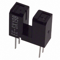
Specifications of EE-SX198
EESX198
EESX198NC
OR631
Available stocks


Related parts for EE-SX198


EE-SX198 Summary of contents
Page 1
... Collector–Emitter saturated volt- age Peak spectral sensitivity wave- length Rising time Falling time 94 EE-SX198 Photomicrosensor (Transmissive) ■ Features • General-purpose model with a 3-mm-wide slot. • PCB mounting type. • High resolution with a 0.5-mm-wide aperture. ■ Absolute Maximum Ratings ( Two, C1 0.3 ...
Page 2
... Relative Light Current vs. Ambi- ent Temperature Characteristics (Typical Ambient temperature Sensing Position Characteristics (Typical (Center of optical axis) Distance d (mm) EE-SX198 Photomicrosensor (Transmissive) Light Current vs. Forward Current Characteristics (Typical Forward current I (mA) F Dark Current vs. Ambient Temperature Characteristics (Typical Ambient temperature Sensing Position Characteristics (Typical) 120 ...