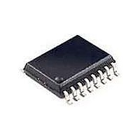
HV9912NG-G Supertex, HV9912NG-G Datasheet

HV9912NG-G
Specifications of HV9912NG-G
Available stocks
Related parts for HV9912NG-G
HV9912NG-G Summary of contents
Page 1
... The HV9912 includes hiccup protection from both short and open circuits, with automatic recovery after the fault condition is cleared. The HV9912 is a pin compatible replacement to Supertex’s HV9911 compatible with existing HV9911 designs which have an input voltage of less than 90V by changing R ...
Page 2
... UVLO V undervoltage lockout threshold RISE DD UVLO V undervoltage lockout hysteresis HYST DD ● Pin Configuration Package Option 16-Lead SOIC 9.90x3.90mm body 1.75mm height (max) 1.27mm pitch HV9912NG-G Value -0.5V to +100V -0.3V to +13.5V Product Marking -0. 0.3V) DD -0. 0.3V) DD -0. 0.3V) DD -0. 0.3V +25°C) ...
Page 3
... OVP falling 280 0 C < T < + 330 -40 C < T < +125 O A COMP = 200 ns DD LIM 600mV step SENSE COMP = 200 ns DD LIM 400mV step SENSE 10 mV --- - MHz 75pF capacitance at OP pin - dB Output open ● Tel: 408-222-8888 ● www.supertex.com HV9912 REF REF; = 300mV; ...
Page 4
... FDBK step from 0 to 900mV; FAULT goes from high to low 300 ns 330pF capacitor at FAULT pin 300 ns 330pF capacitor at FAULT pin 900 ns --- - µA --- 100 µA --- 2. 50µ SLOPE SC < +125 C are guaranteed by design and characterization ● Tel: 408-222-8888 ● www.supertex.com HV9912 = GND REF 400mA; = 1.0kΩ ...
Page 5
... IC if the voltage at the VDD pin falls below the UVLO threshold. 1235 Bordeaux Drive, Sunnyvale, CA 94089 rising 4.5V falling OVPD SCD One Shot PWMD GND ● Tel: 408-222-8888 ● www.supertex.com HV9912 REF GATE FAULT OVP SYNC RT ...
Page 6
... SYNC pin is considered fault tolerant 1235 Bordeaux Drive, Sunnyvale, CA 94089 6 is less than VIN . In such cases, the IC will oscil- STOP and GND will program the T sets the current which charges T T ≈ 18pF S T ● Tel: 408-222-8888 ● www.supertex.com HV9912 . STOP (Eqn. 3) ...
Page 7
... LEDs. This minimizes the effect of the capacitor on the PWM dimming response of the converter. However, in the case of a boost converter, the output current is dis- 1235 Bordeaux Drive, Sunnyvale, CA 94089 7 CLIM should be reduced till CS ● Tel: 408-222-8888 ● www.supertex.com HV9912 is greater than ...
Page 8
... HV9912 is 10μs. POR V IN POR Pull-up Pull-down Gm control with 5.0µA with 5.0µA 5.0V 1.0V t POR FLT t DELAY Fig. 2 Waveforms During Startup ● Tel: 408-222-8888 ● www.supertex.com HV9912 amplifier and M ), the start-up C (Eqn. 8) can Z < 100kΩ). The Z ...
Page 9
... Note that the number of hiccup cycles might be more than two. 1235 Bordeaux Drive, Sunnyvale, CA 94089 case of a persistent open circuit condition, this t ≈ 0 OVP1 OVP2 COMP t ≈ HICCUP1 C Z 5µ ≈ HICCUP2 5µA ● Tel: 408-222-8888 ● www.supertex.com HV9912 OVP1 (Eqn. 10) (Eqn. 11) (Eqn. 12) ...
Page 10
... LEDs. To get zero LED current, the PWMD input has to be pulled to GND. OVP ON LED string reconnects OVP OFF HICCUP1 Fig. 4 Open Circuit Protection 1235 Bordeaux Drive, Sunnyvale, CA 94089 10 LED string voltage t HICCUP2 ● Tel: 408-222-8888 ● www.supertex.com HV9912 ...
Page 11
... The voltage at this pin sets the output current level. The current reference can be set using a resistor 15 IREF divider from the REF pin. 16 FDBK This pin provides output current feedback to the HV9912 by using a current sense resistor. ● 1235 Bordeaux Drive, Sunnyvale, CA 94089 11 ● Tel: 408-222-8888 ● www.supertex.com HV9912 ...
Page 12
... JEDEC Registration MS-012, Variation AC, Issue E, Sept. 2005. * This dimension is not specified in the JEDEC drawing. Drawings are not to scale. Supertex Doc. #: DSPD-16SONG, Version G041309. (The package drawing(s) in this data sheet may not reflect the most current specifications. For the latest package outline information go to http://www.supertex.com/packaging.html.) does not recommend the use of its products in life support applications, and will not knowingly sell them for use in such applications unless it receives Supertex inc ...


