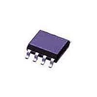
HV9930LG-G Supertex, HV9930LG-G Datasheet - Page 4

HV9930LG-G
Manufacturer Part Number
HV9930LG-G
Description
LED Drivers Hysteric Boost-Buck
Manufacturer
Supertex
Datasheet
1.HV9930LG-G.pdf
(7 pages)
Specifications of HV9930LG-G
Operating Supply Voltage
8 V to 200 V
Maximum Supply Current
1000 uA
Maximum Power Dissipation
630 mW
Maximum Operating Temperature
+ 85 C
Mounting Style
SMD/SMT
Package / Case
SOIC-8 Narrow
Minimum Operating Temperature
- 40 C
Lead Free Status / RoHS Status
Lead free / RoHS Compliant
Functional Block Diagram
Functional Description
Power Topology
The HV9930 is optimized to drive a continuous conduction
mode (CCM) boost-buck DC/DC converter topology com-
monly referred to as “Ćuk converter” (see Typical Application
Circuit on page 1). This power converter topology offers nu-
merous advantages useful for driving high-brightness light
emitting diodes (HB LED). These advantages include step-
up or step-down voltage conversion ratio and low input and
output current ripple. The input and the output inductors can
also share a common core. The output load is decoupled
from the input voltage with a capacitor making the driver in-
herently failure-safe for the output load.
The HV9930 offers a simple and effective control technique
for use with a boost-buck LED driver. It uses two hysteretic
mode controllers – one for the input and one for the output.
The outputs of these two hysteretic comparators are AND
together, and used to drive the external FET. This control
scheme gives accurate current control and constant output
current in the presence of input voltage transients without
the need for complicated loop design.
Input Voltage Regulator
The HV9930 can be powered directly from its VIN pin that
takes a voltage from 8 to 200V. When a voltage is applied
at the VIN pin, the HV9930 tries to maintain a constant 7.5V
(typ) at the VDD pin. The regulator also has a built in under-
voltage lockout which shuts off the IC if the voltage at the
VDD pin falls below the UVLO threshold.
The VDD pin must be bypassed by a low ESR capacitor
Supertex inc.
PWMD
CS1
CS2
VIN
1235 Bordeaux Drive, Sunnyvale, CA 94089
100mV
Regulator
Output
Comparator
HV9930
Input
Comparator
4
(≥0.1µF) to provide a low impedance path for the high fre-
quency current of the output gate driver.
The IC can also be operated by supplying a voltage at the
VDD pin greater than the internally regulated voltage. This
will turn off the internal linear regulator and the IC will func-
tion by drawing power from the external voltage source con-
nected to the VDD pin.
In case of input transients that reduce the input voltage be-
low 8.0V (like cold crank condition in an automotive system),
the VIN pin of the HV9930 can be connected to the drain of
the MOSFET through a diode. Since the drain of the FET is
at a voltage equal to the sum of the input and output voltag-
es, the IC will still be operational when the input goes below
8.0V. In these cases, a larger capacitor is needed to the VDD
pin to supply power to the IC when the MOSFET is on.
Reference
An internally trimmed voltage reference of 1.25V (± 3%) is
provided at the REF pin. The reference can supply a maxi-
mum output current of 1.0mA to drive external circuitry.This
reference can be used to set the current thresholds of the two
comparators as shown in the Typical Application Circuit.
Current Comparators
The HV9930 features two identical comparators with a built-
in 100mV hysteresis. When the GATE is low, the inverting
terminal is connected to 100mV and when the GATE is high,
it is connected to GND. One comparator is used for the input
current control and the other for the output current control.
1.25V
Tel: 408-222-8888
7.5V
VDD
GATE
REF
GND
www.supertex.com
HV9930


