HV9961NG-G Supertex, HV9961NG-G Datasheet
HV9961NG-G
Specifications of HV9961NG-G
Available stocks


Related parts for HV9961NG-G


HV9961NG-G Summary of contents
Page 1
... Supertex inc. LED Driver with Average-Mode Features ► Fast average current control ► Programmable constant off-time switching ► Linear dimming input ► PWM dimming input ► Output short circuit protection with skip mode ► Ambient operating temperature -40 ► Pin-compatible with the HV9910B Applications ► ...
Page 2
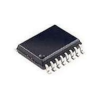
... Denotes the specifications which apply over the full operating ambient temperature range of -40°C < T Supertex inc. Pin Description 16-Lead SOIC 9.90x3.90mm body 1.75mm height (max) 1.27mm pitch HV9961NG-G GATE Product Marking Value -0.5V to +470V Package may or may not include the following marks 12V -0 ...
Page 3
... Current limit delay CS-to-GATE DELAY T Short circuit hiccup time HICCUP T Minimum on-time (short circuit) ON(min) Notes: * Denotes the specifications which apply over the full operating ambient temperature range of -40°C < Guaranteed by design. Supertex inc. (Specifications are 25° 12V Min Typ - 7.25 7. ...
Page 4
... RISE t GATE output fall time FALL Notes: * Denotes the specifications which apply over the full operating ambient temperature range of -40°C < Guaranteed by design. Functional Block Diagram VIN LD CS GND HV9961 Supertex inc. (Specifications are 25° 12V Min Typ - 8 0.165 ...
Page 5
... IN sively complex and expensive in the offline AC or other high- voltage DC applications. The HV9961 employs Supertex’ proprietary control scheme, achieving fast and very accurate control of average current in the buck inductor through sensing the switch current only. No compensation of the current control loop is required. The LED current response to PWMD input is similar to that of the HV9910B ...
Page 6
... Fig.3. Typical linear dimming response of an HV9961 LED driver The linear dimming input could also be used for “mixed- mode” dimming to expand the dimming ratio. In such case a Supertex inc. pulse-width modulated signal of a measured amplitude be- low 1.5V should be applied at LD. Input Voltage Regulator The HV9961 can be powered directly from an 8 ...
Page 7
... Supertex inc. The rising and falling edges are limited by the current slew rate in the inductor. The first switching cycle is terminated upon reaching the 275mV (V cuit is further reaching its steady-state within 3~4 switching cycles regardless of the switching frequency. Function Description VIN This pin is the input ...
Page 8
... Symbol A A1 MIN 1.35* 0.10 Dimension NOM - - (mm) MAX 1.75 0.25 JEDEC Registration MS-012, Variation AA, Issue E, Sept. 2005. * This dimension is not specified in the JEDEC drawing. Drawings are not to scale. Supertex Doc. #: DSPD-8SOLGTG, Version I041309. Supertex inc Note 1 Seating Plane 1.25 0.31 4 ...
Page 9
... JEDEC Registration MS-012, Variation AC, Issue E, Sept. 2005. * This dimension is not specified in the JEDEC drawing. Drawings are not to scale. Supertex Doc. #: DSPD-16SONG, Version G041309. (The package drawing(s) in this data sheet may not reflect the most current specifications. For the latest package outline information go to http://www.supertex.com/packaging.html.) does not recommend the use of its products in life support applications, and will not knowingly sell them for use in such applications unless it receives Supertex inc ...