TSL2014 TAOS, TSL2014 Datasheet - Page 7

TSL2014
Manufacturer Part Number
TSL2014
Description
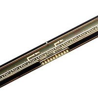
Photodiodes Linear Array 200 DPI
Manufacturer
TAOS
Type
Linear Sensor Arrayr
Datasheet
1.TSL2014.pdf
(10 pages)
Specifications of TSL2014
Peak Wavelength
1000 nm
Maximum Rise Time
500 ns
Maximum Fall Time
500 ns
Maximum Operating Temperature
+ 70 C
Minimum Operating Temperature
0 C
Product
Photodiode
Lead Free Status / RoHS Status
Lead free / RoHS Compliant
Integration Time
The LUMENOLOGY r Company
The integration time of the linear array is the period during which light is sampled and charge accumulates on
each pixel’s integrating capacitor. The flexibility to adjust the integration period is a powerful and useful feature
of the TAOS TSL2xx linear array family. By changing the integration time, a desired output voltage can be
obtained on the output pin while avoiding saturation for a wide range of light levels.
Each pixel of the linear array consists of a light-sensitive photodiode. The photodiode converts light intensity
to a voltage. The voltage is sampled on the Sampling Capacitor by closing switch S2 (position 1) (see the
functional block diagram on page 1). Logic controls the resetting of the Integrating Capacitor to zero by closing
switch S1 (position 2).
At SI input (Start Integration), pixel 1 is accessed. During this event, S2 moves from position 1 (sampling) to
position 3 (holding). This holds the sampled voltage for pixel 1. Switch S1 for pixel 1 is then moved to position
2. This resets (clears) the voltage previously integrated for that pixel so that pixel 1 is now ready to start a new
integration cycle. When the next clock period starts, the S1 switch is returned to position 1 to be ready to
start integrating again. S2 is returned to position 1 to start sampling the next light integration. Then the next pixel
starts the same procedure. The integration time is the time from a specific pixel read to the next time that pixel
is read again. If either the clock speed or the time between successive SI pulses is changed, the integration time
will vary. After the final (n
A new SI pulse can occur on the (n+1) clock causing a new cycle of integration/output to begin. Note that the
time between successive SI pulses must not exceed the maximum integration time of 100 msec.
The minimum integration time for any given array is determined by time required to clock out all the pixels in
the array and the time to discharge the pixels. The time required to discharge the pixels is a constant. Therefore,
the minimum integration period is simply a function of the clock frequency and the number of pixels in the array.
A slower clock speed increases the minimum integration time and reduces the maximum light level for saturation
on the output. The minimum integration time shown in this data sheet is based on the maximum clock frequency
of 5 MHz.
The minimum integration time can be calculated from the equation:
where:
In the case of the TSL2014, the minimum integration time would be:
It is important to note that not all pixels will have the same integration time if the clock frequency is varied while
data is being output.
n
is
the number of pixels
T
T
int(min)
int(min)
th
) pixel in the array is read on the output, the output goes into a high-impedance mode.
+
+ 200 ns
maximum clock frequency
APPLICATION INFORMATION
r
448 + 179.2ns
www.taosinc.com
1
n
896 y 1 LINEAR SENSOR ARRAY
r
Copyright E 2007, TAOS Inc.
TAOS040B − MAY 2007
TSL2014
7


