A000046 Arduino, A000046 Datasheet - Page 71
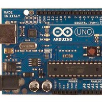
A000046
Manufacturer Part Number
A000046
Description
MCU, MPU & DSP Development Tools Uno
Manufacturer
Arduino
Series
-r
Type
MCUr
Specifications of A000046
Processor To Be Evaluated
ATmega328
Interface Type
USB, I2C, SPI
Dimensions
2.7 in x 2.1 in
Operating Supply Voltage
5 V
Contents
Board
Lead Free Status / RoHS Status
Lead free / RoHS Compliant
For Use With/related Products
ATmega328


12.2
12.2.1
8161D–AVR–10/09
Register Description
EICRA – External Interrupt Control Register A
The External Interrupt Control Register A contains control bits for interrupt sense control.
• Bit 7..4 – Res: Reserved Bits
These bits are unused bits in the ATmega48PA/88PA/168PA/328P, and will always read as
zero.
• Bit 3, 2 – ISC11, ISC10: Interrupt Sense Control 1 Bit 1 and Bit 0
The External Interrupt 1 is activated by the external pin INT1 if the SREG I-flag and the corre-
sponding interrupt mask are set. The level and edges on the external INT1 pin that activate the
interrupt are defined in
edges. If edge or toggle interrupt is selected, pulses that last longer than one clock period will
generate an interrupt. Shorter pulses are not guaranteed to generate an interrupt. If low level
interrupt is selected, the low level must be held until the completion of the currently executing
instruction to generate an interrupt.
Table 12-1.
• Bit 1, 0 – ISC01, ISC00: Interrupt Sense Control 0 Bit 1 and Bit 0
The External Interrupt 0 is activated by the external pin INT0 if the SREG I-flag and the corre-
sponding interrupt mask are set. The level and edges on the external INT0 pin that activate the
interrupt are defined in
edges. If edge or toggle interrupt is selected, pulses that last longer than one clock period will
generate an interrupt. Shorter pulses are not guaranteed to generate an interrupt. If low level
interrupt is selected, the low level must be held until the completion of the currently executing
instruction to generate an interrupt.
Table 12-2.
Bit
(0x69)
Read/Write
Initial Value
ISC11
ISC01
0
0
1
1
0
0
1
1
Interrupt 1 Sense Control
Interrupt 0 Sense Control
ISC10
ISC00
R
7
–
0
0
1
0
1
0
1
0
1
Table
Table
Description
Description
The low level of INT1 generates an interrupt request.
Any logical change on INT1 generates an interrupt request.
The falling edge of INT1 generates an interrupt request.
The rising edge of INT1 generates an interrupt request.
The low level of INT0 generates an interrupt request.
Any logical change on INT0 generates an interrupt request.
The falling edge of INT0 generates an interrupt request.
The rising edge of INT0 generates an interrupt request.
R
6
–
0
12-1. The value on the INT1 pin is sampled before detecting
12-2. The value on the INT0 pin is sampled before detecting
ATmega48PA/88PA/168PA/328P
R
5
–
0
R
4
–
0
ISC11
R/W
3
0
ISC10
R/W
2
0
ISC01
R/W
1
0
ISC00
R/W
0
0
EICRA
71
Related parts for A000046
Image
Part Number
Description
Manufacturer
Datasheet
Request
R

Part Number:
Description:
Daughter Cards & OEM Boards ARDUINO UNO PROTO PCB REV 3
Manufacturer:
Arduino
Part Number:
Description:
Daughter Cards & OEM Boards ARDUINO SHIELD PROTO KIT REV 3
Manufacturer:
Arduino
Part Number:
Description:
Daughter Cards & OEM Boards ARDUINO MEGA PROTO KIT REV 3
Manufacturer:
Arduino
Part Number:
Description:
Daughter Cards & OEM Boards ARDUINO MEGA PROTO PCB REV 3
Manufacturer:
Arduino
Part Number:
Description:
Development Boards & Kits - AVR ARDUINO STARTER KIT W/ UNO REV3
Manufacturer:
Arduino
Part Number:
Description:
RF Development Tools ARDUINO SHIELD WIRELESS PROTO
Manufacturer:
Arduino
Datasheet:
Part Number:
Description:
RF Development Tools ARDUINO SHIELD WIRELESS WITH SD
Manufacturer:
Arduino
Datasheet:

Part Number:
Description:
Development Software Getting started w/Arduino
Manufacturer:
Arduino

Part Number:
Description:
Ethernet Modules & Development Tools Ethernet Shield for Arduino
Manufacturer:
Arduino

Part Number:
Description:
MCU, MPU & DSP Development Tools LilyPad Arduino Main Board
Manufacturer:
Arduino

Part Number:
Description:
ARDUINO NANO Board
Manufacturer:
Arduino
Datasheet:
Part Number:
Description:
Ethernet Modules & Development Tools ETHERNET SHEILD PoE FOR ARDUINO
Manufacturer:
Arduino
Datasheet:

Part Number:
Description:
ATMEGA328 MCU IC W/ Arduino UNO Bootloader
Manufacturer:
Arduino
Datasheet:
Part Number:
Description:
Memory Cards MICRO SD CARD 1GB WITH SD ADAPTER
Manufacturer:
Arduino