MAX98302ETD+T Maxim Integrated Products, MAX98302ETD+T Datasheet - Page 9
MAX98302ETD+T
Manufacturer Part Number
MAX98302ETD+T
Description
Audio Amplifiers STEREO 2W CLASS D AMP
Manufacturer
Maxim Integrated Products
Datasheet
1.MAX98302ETD.pdf
(13 pages)
Specifications of MAX98302ETD+T
Product
Class-D
Output Power
2.4 W
Common Mode Rejection Ratio (min)
62 dB
Thd Plus Noise
0.04 %
Supply Current
2.25 mA
Maximum Power Dissipation
1951 mW
Maximum Operating Temperature
+ 85 C
Mounting Style
SMD/SMT
Output Type
2-Channel Stereo
Package / Case
TDFN-14
Amplifier Class
D
No. Of Channels
2
Supply Voltage Range
2.6V To 5.5V
Thd + N
0.04% @ 0.5W, 8ohm, VPVDD=5V%
Load Impedance
4ohm
Operating Temperature Range
-40°C To +85°C
Rohs Compliant
Yes
Lead Free Status / RoHS Status
Lead free / RoHS Compliant


The input-coupling capacitor (C
the amplifier’s internal input resistance (R
highpass filter that removes the DC bias from the incom-
ing signal. These capacitors allow the amplifier to bias
the signal to an optimum DC level.
Assuming zero-source impedance with a gain setting of
A
with a gain setting of A
with a gain setting of A
where f
tors with adequately low-voltage coefficients for best
low-frequency THD performance.
V
= 12dB, 15dB, or 18dB, C
-3dB
is the -3dB corner frequency. Use capaci-
_______________________________________________________________________________________
C
C
C
IN
IN
IN
V
V
=
=
=
= 9dB, C
= 6dB, C
f
f
f
−
−
−
5.7
3dB
3dB
3dB
8
4
IN
[ F]
[ F]
[ F]
is:
µ
µ
µ
IN
IN
IN
), in conjunction with
is:
is:
Input Filtering
Stereo 2.4W Class D Amplifier
IN
), forms a
Proper layout and grounding are essential for optimum
performance. Good grounding improves audio perfor-
mance and prevents switching noise from coupling into
the audio signal.
Use wide, low-resistance output traces. As load imped-
ance decreases, the current drawn from the device
outputs increase. At higher current, the resistance of
the output traces decrease the power delivered to the
load. For example, if 2W is delivered from the speaker
output to a 4I load through a 100mI trace, 49mW is
consumed in the trace. If power is delivered through a
10mI trace, only 5mW is consumed in the trace. Wide
output, supply, and ground traces also improve the
power dissipation of the device.
The MAX98302 is inherently designed for excellent RF
immunity. For best performance, add ground fills around
all signal traces on top or bottom PCB planes.
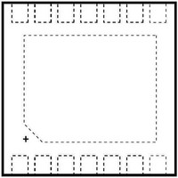
The MAX98302 TDFN-EP package features an exposed
thermal pad on its underside. This pad lowers the pack-
age’s thermal resistance by providing a heat conduction
path from the die to the PCB. Connect the exposed
thermal pad to the ground plane by using a large pad
and multiple vias.
Layout and Grounding
9
Related parts for MAX98302ETD+T
Image
Part Number
Description
Manufacturer
Datasheet
Request
R

Part Number:
Description:
Stereo 2.4w Class D Amplifier
Manufacturer:
Maxim Integrated Products, Inc.
Datasheet:

Part Number:
Description:
MAX7528KCWPMaxim Integrated Products [CMOS Dual 8-Bit Buffered Multiplying DACs]
Manufacturer:
Maxim Integrated Products
Datasheet:
Part Number:
Description:
Single +5V, fully integrated, 1.25Gbps laser diode driver.
Manufacturer:
Maxim Integrated Products
Datasheet:
Part Number:
Description:
Single +5V, fully integrated, 155Mbps laser diode driver.
Manufacturer:
Maxim Integrated Products
Datasheet:
Part Number:
Description:
VRD11/VRD10, K8 Rev F 2/3/4-Phase PWM Controllers with Integrated Dual MOSFET Drivers
Manufacturer:
Maxim Integrated Products
Datasheet:
Part Number:
Description:
Highly Integrated Level 2 SMBus Battery Chargers
Manufacturer:
Maxim Integrated Products
Datasheet:
Part Number:
Description:
Current Monitor and Accumulator with Integrated Sense Resistor; ; Temperature Range: -40°C to +85°C
Manufacturer:
Maxim Integrated Products
Part Number:
Description:
TSSOP 14/A°/RS-485 Transceivers with Integrated 100O/120O Termination Resis
Manufacturer:
Maxim Integrated Products
Part Number:
Description:
TSSOP 14/A°/RS-485 Transceivers with Integrated 100O/120O Termination Resis
Manufacturer:
Maxim Integrated Products
Part Number:
Description:
QFN 16/A°/AC-DC and DC-DC Peak-Current-Mode Converters with Integrated Step
Manufacturer:
Maxim Integrated Products
Part Number:
Description:
TDFN/A/65V, 1A, 600KHZ, SYNCHRONOUS STEP-DOWN REGULATOR WITH INTEGRATED SWI
Manufacturer:
Maxim Integrated Products
Part Number:
Description:
Integrated Temperature Controller f
Manufacturer:
Maxim Integrated Products
Part Number:
Description:
SOT23-6/I°/45MHz to 650MHz, Integrated IF VCOs with Differential Output
Manufacturer:
Maxim Integrated Products
Part Number:
Description:
SOT23-6/I°/45MHz to 650MHz, Integrated IF VCOs with Differential Output
Manufacturer:
Maxim Integrated Products