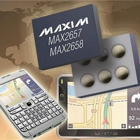
MAX2657EWT+T Maxim Integrated Products, MAX2657EWT+T Datasheet

MAX2657EWT+T
Specifications of MAX2657EWT+T
Related parts for MAX2657EWT+T
MAX2657EWT+T Summary of contents
Page 1
... Wide Supply Voltage Range: 1.6V to 3.3V ♦ Low Bill of Materials: One Inductor, Two Capacitors ♦ Small Footprint: 0.86mm x 1.26mm ♦ Thin Profile: 0.65mm ♦ 0.4mm-Pitch Wafer-Level Package (WLP) Applications PART MAX2657EWT+T MAX2658EWT+T + Denotes a lead(Pb)-free/RoHS-compliant package Tape and reel. Pin Configuration/Typical Application Circuit + MAX2657 MAX2658 ...
Page 2
GPS/GNSS Low-Noise Amplifiers ABSOLUTE MAXIMUM RATINGS V to GND ...........................................................-0.3V to +3.6V CC Other Pins to GND .................-0. Operating V Maximum RF Input Power ...............................................+5dBm Continuous Power Dissipation (T = +70°C) A 6-Bump WLP (derates 10.5mW/°C above +70°C) ...
Page 3
AC ELECTRICAL CHARACTERISTICS (continued) (MAX2657/MAX2658 EV kit 1.6V to 3.3V +25°C, unless otherwise noted.) (Note 2) A PARAMETER Input 1dB Compression point (Note 5) Input Return Loss Output Return Loss Reverse Isolation Note 2: ...
Page 4
GPS/GNSS Low-Noise Amplifiers (MAX2657/MAX2658 EV kit. Typical values are at V OUTPUT RETURN LOSS vs. FREQUENCY 0 -5 MAX2657 -10 MAX2658 -15 -20 -25 500 1000 1500 2000 FREQUENCY (MHz) MAX2657 OUT-OF-BAND IIP3 vs. SUPPLY VOLTAGE AND TEMPERATURE (TONE 1 ...
Page 5
EV kit. Typical values are at V MAX2657 INPUT P1dB COMPRESSION vs. SUPPLY VOLTAGE AND TEMPERATURE -11 -12 -13 +85˚C -14 +25˚C -15 -16 -40˚C -17 -18 1.6 1.8 2.0 2.2 2.4 2.6 SUPPLY VOLTAGE (V) _______________________________________________________________________________________ GPS/GNSS Low-Noise ...
Page 6
GPS/GNSS Low-Noise Amplifiers BUMP NAME SHDN A1 Shutdown Input. A logic-low disables the device. A2 RFOUT RF Output. RFOUT is internally matched to 50Ω and incorporates an internal DC-blocking capacitor. B1 RFIN RF Input. Requires a DC-blocking capacitor and external ...
Page 7
Table 2. MAX2658 Typical S-Parameter Values and K-Factor S11 FREQ. S11 MAG PHASE (MHz) (dB) (Degrees) 1000 -3.0 -57.0 1100 -3.3 -58.2 1200 -3.5 -60.0 1300 -3.8 -62.3 1400 -4.3 -63.3 1500 -4.9 -62.0 1575 -5.3 -59.7 1600 -5.4 -58.5 ...
Page 8
... Maxim cannot assume responsibility for use of any circuitry other than circuitry entirely embodied in a Maxim product. No circuit patent licenses are implied. Maxim reserves the right to change the circuitry and specifications without notice at any time. 8 _____________________Maxim Integrated Products, 120 San Gabriel Drive, Sunnyvale, CA 94086 408-737-7600 © 2009 Maxim Integrated Products ...


