DS4402N+ Maxim Integrated Products, DS4402N+ Datasheet - Page 6

DS4402N+
Manufacturer Part Number
DS4402N+
Description
DAC (D/A Converters) IC DAC 2CH I2C ADJ justable Sink-Source
Manufacturer
Maxim Integrated Products
Datasheet
1.DS4402NTR.pdf
(9 pages)
Specifications of DS4402N+
Resolution
5 bit
Interface Type
Serial (I2C)
Supply Voltage (max)
5.5 V
Supply Voltage (min)
2.7 V
Maximum Operating Temperature
+ 85 C
Mounting Style
SMD/SMT
Minimum Operating Temperature
- 40 C
Number Of Converters
2
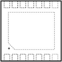
Package / Case
TDFN EP
Lead Free Status / RoHS Status
Lead free / RoHS Compliant
To control the DS4402/DS4404’s current sources, write
to the memory addresses listed in Table 2.
Table 2. Memory Addresses
The format of each output control register is given by:
Where:
Example: I
value of 92h. Calculate the value of external resistance
required, and the magnitude of the output current with
this register setting.
The MSB of the output register is 1, so the output is
sourcing the value corresponding to position 12h (18
decimal). The magnitude of the output current is equal to:
Two/Four-Channel, I
*Only for DS4404.
6
BIT
MSB
D
S
X
S
X
______________________________________________________________________
MEMORY ADDRESS
(HEXADECIMAL)
Reserved
Sign Bit
R
NAME
Data
FS
X
FS0
FAh*
FBh*
= (V
F8h
F9h
= 800µA, and register F8h is written to a
800µA x (18 / 31) = 465µA
REF
Determines if DAC sources
or sinks current. For sink
S = 0, for source S = 1.
Reserved. Both bits read
zero.
5-Bit Data Word Controlling
DAC Output. Setting 00000b
outputs zero current
regardless of the state of the
sign bit.
X
/ 800µA) x (31 / 4) = 11.9kΩ
D
FUNCTION
4
Memory Organization
D
3
CURRENT SOURCE
D
2
OUT2*
OUT3*
OUT0
OUT1
POWER-ON
D
DEFAULT
1
00000b
00b
2
0b
LSB
C Adjustable Current DAC
D
0
The following terminology is commonly used to describe
I
Master Device: The master device controls the slave
devices on the bus. The master device generates SCL
clock pulses, START and STOP conditions.
Slave Devices: Slave devices send and receive data
at the master’s request.
Bus Idle or Not Busy: Time between STOP and START
conditions when both SDA and SCL are inactive and in
their logic-high states. When the bus is idle it often initi-
ates a low-power mode for slave devices.
START Condition: A START condition is generated by
the master to initiate a new data transfer with a slave.
Transitioning SDA from high to low while SCL remains
high generates a START condition. See Figure 3 for
applicable timing.
STOP Condition: A STOP condition is generated by the
master to end a data transfer with a slave. Transitioning
SDA from low to high while SCL remains high generates
a STOP condition. See Figure 3 for applicable timing.
Repeated START Condition: The master can use a
repeated START condition at the end of one data trans-
fer to indicate that it will immediately initiate a new data
transfer following the current one. Repeated STARTs are
commonly used during read operations to identify a spe-
cific memory address to begin a data transfer. A repeat-
ed START condition is issued identically to a normal
START condition. See Figure 3 for applicable timing.
Bit Write: Transitions of SDA must occur during the low
state of SCL. The data on SDA must remain valid and
unchanged during the entire high pulse of SCL, plus the
setup and hold time requirements (Figure 3). Data is
shifted into the device during the rising edge of the SCL.
Bit Read: At the end of a write operation, the master
must release the SDA bus line for the proper amount of
setup time (Figure 3) before the next rising edge of SCL
during a bit read. The device shifts out each bit of data
on SDA at the falling edge of the previous SCL pulse
and the data bit is valid at the rising edge of the current
SCL pulse. Remember that the master generates all
SCL clock pulses, including when it is reading bits from
the slave.
2
C data transfers:
I
2
C Serial Interface Description
I
2
C Definitions


