ZXMP6A17E6TA Diodes Inc, ZXMP6A17E6TA Datasheet
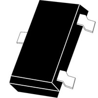
MOSFET Small Signal P-Ch 60 Volt 3.0A

ZXMP6A17E6TA

Manufacturer Part Number
ZXMP6A17E6TA
Description
MOSFET Small Signal P-Ch 60 Volt 3.0A
Manufacturer
Diodes Inc
Datasheet

Specifications of ZXMP6A17E6TA

Minimum Operating Temperature
- 55 C
Configuration
Single Quad Drain
Transistor Polarity
P-Channel
Resistance Drain-source Rds (on)
0.125 Ohm @ 10 V
Drain-source Breakdown Voltage
60 V
Gate-source Breakdown Voltage
+/- 20 V
Continuous Drain Current
3 A
Power Dissipation
1700 mW
Maximum Operating Temperature
+ 150 C
Mounting Style
SMD/SMT
Package / Case
SOT-23
Lead Free Status / RoHS Status
Lead free / RoHS Compliant
Lead Free Status / RoHS Status
Lead free / RoHS Compliant

Available stocks

Company
Part Number
Manufacturer
Quantity
Price
Part Number:
ZXMP6A17E6TA
Manufacturer:
ZETEX
Quantity:
21 000
Part Number:
ZXMP6A17E6TA
Manufacturer:
NS
Quantity:
41
Part Number:
ZXMP6A17E6TA
Manufacturer:
DIODES
Quantity:
6 000
Part Number:
ZXMP6A17E6TA
Manufacturer:
ZETEX/DIODES
Quantity:
20 000
Company:
Part Number:
ZXMP6A17E6TA
Quantity:
5 000
Company:
Part Number:
ZXMP6A17E6TA
Quantity:
3 067
Ordering Information
Marking Information
Product Summary
Description and Applications
This MOSFET has been designed to minimize the on-state resistance
and yet maintain superior switching performance, making it ideal for
high efficiency power management applications.
Notes:
ZXMP6A17E6
Document Number: DS33589 Rev. 2 - 2
DC-DC Converters
Power management functions
Disconnect switches
Motor control
ZXMP6A17E6TA
V
(BR)DSS
-60V
Product
1. No purposefully added lead
2. Diodes Inc's "Green" policy can be found on our website at http://www.diodes.com.
3. For packaging details, go to our website at http://www.diodes.com.
190mΩ @ V
Top View
SOT-26
125mΩ @ V
R
DS(on)
(Note 3)
GS
GS
Max
= -4.5V
= -10V
Marking
6A17
T
(Note 5)
A
6A17
I
-3.0 A
-2.4 A
D
= 25°C
G
D
D
Max
Reel size (inches)
www.diodes.com
Pin Out - Top View
1 of 8
7
Features and Benefits
Mechanical Data
6A17 = Product Type Marking Code
60V P-CHANNEL ENHANCEMENT MODE MOSFET
Low on-resistance
Fast switching speed
Low threshold
Low gate drive
Low input capacitance
“Lead Free”, RoHS Compliant (Note 1)
Halogen and Antimony Free. "Green" Device (Note 2)
Qualified to AEC-Q101 Standards for High Reliability
Case: SOT-26
Case Material: Molded Plastic, UL Flammability Classification
Rating 94V-0
Moisture Sensitivity: Level 1 per J-STD-020
Terminals: Finish - Matte Tin annealed over Copper lead frame.
Solderable per MIL-STD-202, Method 208
Weight: 0.018 grams (approximate)
D
D
S
Tape width (mm)
Diodes Incorporated
A Product Line of
8
G
Equivalent Circuit
D
S
ZXMP6A17E6
Quantity per reel
3,000
© Diodes Incorporated
December 2010

Related parts for ZXMP6A17E6TA

ZXMP6A17E6TA Summary of contents

Page 1

... Motor control SOT-26 Top View Ordering Information (Note 3) Product Marking ZXMP6A17E6TA 6A17 Notes purposefully added lead 2. Diodes Inc's "Green" policy can be found on our website at http://www.diodes.com. 3. For packaging details our website at http://www.diodes.com. Marking Information ZXMP6A17E6 Document Number: DS33589 Rev ...

Page 2

... P D (Note 5) (Note 4) R θ JA (Note STG www.diodes.com A Product Line of Diodes Incorporated ZXMP6A17E6 Value Unit -60 V ±20 V -3.0 -2.4 A -2.3 -13.6 A -2.5 A -13.6 A Value Unit 1.1 8.8 W mW/°C 1.92 15.4 113 °C/W 65 °C -55 to 150 December 2010 © Diodes Incorporated ...

Page 3

... Single Pulse D=0.05 D=0 100 1k 100µ Pulse Power Dissipation www.diodes.com A Product Line of Diodes Incorporated ZXMP6A17E6 100 125 150 Temperature (°C) Derating Curve Single Pulse T =25°C amb 1m 10m 100m 1 10 100 1k Pulse Width (s) December 2010 © Diodes Incorporated ...

Page 4

... GS D Ω 0.190 V = -4.5V -1. ⎯ -15V -2. -0. -2A ⎯ -1.7A, di/dt = 100A/μs F ⎯ nC ⎯ -30V ⎯ 1MHz ⎯ pF ⎯ -5.0V GS ⎯ -30V DS ⎯ -10V I = -2. ⎯ nC ⎯ ns ⎯ -30V -10V DD GS ⎯ ≅ 6.0Ω -1A ⎯ ns December 2010 © Diodes Incorporated ...

Page 5

... Source-Drain Diode Forward Voltage www.diodes.com A Product Line of Diodes Incorporated ZXMP6A17E6 5V 10V 4.5V 3. Drain-Source Voltage (V) DS Output Characteristics V = -10V 2. DS(on GS(th -250uA 100 150 Tj Junction Temperature (° 150° 25° 0.4 0.6 0.8 1.0 1.2 -V Source-Drain Voltage (V) SD December 2010 © Diodes Incorporated ...

Page 6

... Charge Gate charge test circuit V DS 90% 10 d(on) t (on) Switching time test circuit www.diodes.com A Product Line of Diodes Incorporated ZXMP6A17E6 I = -2. -30V Charge (nC) Current regulator 50k 12V 0.2 F Same as D.U D.U Pulse width 1 S Duty factor 0.1% December 2010 © Diodes Incorporated 18 ...

Page 7

... C 2.70 3.00 2.80 ⎯ ⎯ D 0.95 H 2.90 3.10 3.00 J 0.013 0.10 0.05 K 1.00 1.30 1.10 L 0.35 0.55 0.40 M 0.10 0.20 0.15 α ⎯ 0° 8° All Dimensions 3.20 G 1.60 X 0.55 Y 0.80 C1 2.40 C2 0.95 December 2010 © Diodes Incorporated ...

Page 8

... Any Customer or user of this document or products described herein in such applications shall assume all risks of such use and will agree to hold Diodes Incorporated and all the companies whose products are represented on Diodes Incorporated website, harmless against all damages. ...

Related keywords