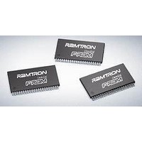
FM22L16-55-TG Ramtron, FM22L16-55-TG Datasheet

FM22L16-55-TG
Specifications of FM22L16-55-TG
Available stocks
Related parts for FM22L16-55-TG
FM22L16-55-TG Summary of contents
Page 1
... This is a product in the pre-production phase of development. Device characterization is complete and Ramtron does not expect to change the specifications. Ramtron will issue a Product Change Notice if any specification changes are made. Rev. 2.0 Apr ...
Page 2
... Input Chip Enable input: The device is selected and a new memory access begins when /CE is low and /ZZ is high. The entire address is latched internally on the falling edge of /CE. Subsequent changes to the A(1:0) address inputs allow page mode operation when /CE is low. ...
Page 3
Functional Truth Table /CE /WE A(16: Change L H Change Change X X Notes: 1) H=Logic High, L=Logic Low, V=Valid Data, X=Don’t ...
Page 4
... Read Operation A read operation begins on the falling edge of /CE. The falling edge of /CE causes the address to be latched and starts a memory read cycle if /WE is high. Data becomes available on the bus after the access time has been satisfied. Once the address has been ...
Page 5
... Precharge Operation The precharge operation is an internal condition in which the state of the memory is being prepared for a new access. Precharge is user-initiated by driving the /CE signal high. It must remain high for at least the minimum precharge time Precharge is also activated by changing the upper addess A(16:2). The current row is first closed prior to accessing the new row ...
Page 6
A flow chart of the entire write protect operation is shown in For example, the following sequence write-protects addresses from 0C000h to 13FFFh ...
Page 7
Figure 4. Sequence to Set Write-Protect Blocks Note: This sequence requires t Figure 5. Sequence to Read Write-Protect Settings Note: This sequence requires t Rev. 2.0 Apr. 2011 ≥ 10ns and address must be stable while /CE is low. AS ...
Page 8
... The /UB and /LB byte select pins are active for both read and write cycles. They may be used to allow the device to be wired as a 256Kx8 memory. The upper and lower data bytes can be tied together and controlled with the byte selects. Individual byte ...
Page 9
Electrical Specifications Absolute Maximum Ratings Symbol Description V Power Supply Voltage with respect Voltage on any signal pin with respect Storage Temperature STG T Lead Temperature (Soldering, 10 seconds) LEAD V Electrostatic ...
Page 10
Read Cycle AC Parameters ( Symbol Parameter t Read Cycle Time RC t Chip Enable Access Time CE t Address Access Time AA t Output Hold Time OH t Page Mode ...
Page 11
... Sleep Mode Exit Time (/ZZ high to 1 ZZEX Notes 1. Slope measured at any point Ramtron cannot test or characterize all V when V is below the level of a transistor threshold voltage. Ramtron strongly recommends that V DD 100ms through the range of 0.4V to 1.0V 2.7V to 3.6V) Data Retention DD Parameter Data Retention ...
Page 12
Page Mode Read Cycle Timing Although sequential column addressing is shown not required. Write Cycle Timing 1 (/WE-Controlled) Write Cycle Timing 2 (/CE-Controlled) CE A(17:0) WE DQ(15:0) UB/LB Rev. 2.0 Apr. 2011 Note: /OE (not shown) is low ...
Page 13
Write Cycle Timing 3 (/CE low) Note: /OE (not shown) is low only to show effect of / pins Page Mode Write Cycle Timing Although sequential column addressing is shown not required. Power Cycle and Sleep ...
Page 14
... XXXXXX= part number, S= speed, P=package RAMTRON XXXXXXX-S-P LLLLLL= lot code, YY=year, WW=work week LLLLLLL YYWW Examples: FM21L16, 60ns access time, “Green”/RoHS TSOP-II package, Lot 6340282, Year 2007, Work Week 31 RAMTRON FM21L16-60-TG 6340282 0731 Rev. 2.0 Apr. 2011 Recommended PCB Footprint 18.41 ...
Page 15
Revision History Revision Date 1.0 9/24/2007 1.1 12/12/2007 1.2 12/22/2009 2.0 4/4/2011 Rev. 2.0 Apr. 2011 Summary Initial release. Added package MSL rating and placeholder for ESD ratings. Lowered I limit. Added UB/LB signals to timing diagrams and added DD ...


