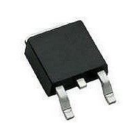
ZLDO1117K25TC Diodes Inc, ZLDO1117K25TC Datasheet - Page 7

ZLDO1117K25TC
Manufacturer Part Number
ZLDO1117K25TC
Description
Low Dropout (LDO) Regulators LDO Regulator IC 2.5V/1A
Manufacturer
Diodes Inc
Datasheet
1.ZLDO1117GTA.pdf
(12 pages)
Specifications of ZLDO1117K25TC
Number Of Outputs
1
Polarity
Positive
Input Voltage Max
18 V
Output Voltage
2.5 V
Output Voltage Tolerance
2 %
Output Type
Fixed
Dropout Voltage (max)
1.3 V
Output Current
1 A
Line Regulation
0.1 %
Load Regulation
5 mV
Maximum Operating Temperature
+ 125 C
Mounting Style
SMD/SMT
Minimum Operating Temperature
- 40 C
Reference Voltage
2.5 V
Package / Case
TO-252-3L
Lead Free Status / RoHS Status
Lead free / RoHS Compliant
Lead Free Status / RoHS Status
Lead free / RoHS Compliant
Available stocks
Company
Part Number
Manufacturer
Quantity
Price
Company:
Part Number:
ZLDO1117K25TC
Manufacturer:
DIODES
Quantity:
36 000
A Product Line of
Diodes Incorporated
ZLDO1117
The device will require an output capacitor of 22µF tantalum or 150µF aluminum electrolytic when the adjust pin is bypassed.
Normally, capacitor values on the order of 100µF are used in the output of many regulators to ensure good load transient
response with large load current changes. Output capacitance can be increased without limit and larger values of output
capacitance further improve stability and transient response.
The curves for Ripple Rejection were generated using an adjustable device with the adjust pin bypassed. These curves will
hold true for all values of output voltage. For proper bypassing, and ripple rejection approaching the values shown, the
impedance of the adjust pin capacitor, at the ripple frequency, should be < R1. R1 is normally in the range of 100Ω to 200Ω.
The size of the required adjust pin capacitor is a function of the input ripple frequency. At 120Hz, with R1 = 100Ω, the adjust
pin capacitor should be >13µF. At 10kHz only 0.16µF is needed.
For fixed voltage devices, and adjustable devices without an adjust pin capacitor, the output ripple will increase as the ratio of
the output voltage to the reference voltage (V
/V
). For example, with the output voltage equal to 5V, the output ripple will
OUT
REF
be increased by the ratio of 5V/1.25V. It will increase by a factor of four. Ripple rejection will be degraded by 12dB from the
value shown on the curve.
ZLDO1117
7 of 12
July 2010
www.diodes.com
© Diodes Incorporated
Document number: Ds32018 Rev. 4 - 2


