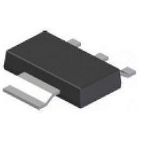
ZLDO1117G50TA Diodes Inc, ZLDO1117G50TA Datasheet - Page 2

ZLDO1117G50TA
Manufacturer Part Number
ZLDO1117G50TA
Description
Low Dropout (LDO) Regulators LDO Regulator IC 5.0V/1A
Manufacturer
Diodes Inc
Datasheet
1.ZLDO1117GTA.pdf
(12 pages)
Specifications of ZLDO1117G50TA
Number Of Outputs
1
Polarity
Positive
Input Voltage Max
18 V
Output Voltage
5 V
Output Voltage Tolerance
2 %
Output Type
Fixed
Dropout Voltage (max)
1.3 V
Output Current
1 A
Line Regulation
0.1 %
Load Regulation
10 mV
Maximum Operating Temperature
+ 125 C
Mounting Style
SMD/SMT
Minimum Operating Temperature
- 40 C
Reference Voltage
5 V
Package / Case
SOT-223-3L
Primary Input Voltage
18V
Output Voltage Fixed
5V
Dropout Voltage Vdo
1.11V
No. Of Pins
3
Voltage Regulator Case Style
SOT-223
Operating Temperature Range
-40°C To +125°C
Svhc
No
Rohs Compliant
Yes
Lead Free Status / RoHS Status
Lead free / RoHS Compliant
Lead Free Status / RoHS Status
Lead free / RoHS Compliant
Available stocks
Company
Part Number
Manufacturer
Quantity
Price
Part Number:
ZLDO1117G50TA
Manufacturer:
DIODES/美台
Quantity:
20 000
Absolute Maximum Ratings
(Semiconductor devices are ESD sensitive and may be damaged by exposure to ESD events. Suitable ESD precautions should be taken when handling and
transporting these devices.)
Operation above the absolute maximum rating may cause device failure.
Operation at the absolute maximum ratings, for extended periods, may reduce device reliability.
Unless otherwise stated voltages specified are relative to the ANODE pin.
These are stress ratings only. Operation outside the absolute maximum ratings may cause device failure.
Recommended Operating Conditions
Package thermal Data
Notes:
ZLDO1117
Document number: Ds32018 Rev. 4 - 2
Thermal Resistance
Junction-to-Ambient, θ
Junction-to-Case, θ
ESD Susceptibility
HBM
MM
1.2
0.8
0.6
0.4
0.2
1
0
Symbol
Symbol
0
T
V
2. ZLDO1117 contains an internal thermal limiting circuit that is designed to protect the regulator in the event that the maximum junction
3. Test condition for SOT223-3L: TA = 27°C, no air flow, device mounted on 2”X2” polyimide PCB, 2 oz copper, 5.6mmX5.6mm pad.
4. Test condition for TO252-3L: TA = 27°C, no air flow, device mounted on 2”X2” polyimide PCB, 1 oz copper, 2cmX2cm pad.
5. Ensures correct operation without entering dropout. Device will continue to operate below this minimum input voltage under dropout conditions.
V
T
T
I
ST
O
IN
IN
J
temperature exceeded. When activated, typically at 150°C, the regulator Output switches off and then back on as the die cools.
J
Safe Operation Area (SOA) Curve
5
JC
Input voltage
Output current
O
Input Supply Voltage (Relative to Ground)
Junction Temperature
Power Dissipation
Storage Temperature
SOA
Human Body Model
Machine Model
JA
perating Junction Temperature Range
SOT223-3L
TO252-3L
SOT223-3L
TO252-3L
Package
10
V
IN
- V
OUT
4
4
3
3
(V)
15
Parameter
Parameter
107
73
16
12
20
www.diodes.com
°C/W
°C/W
Unit
2 of 12
25
See SOA Curve
0.01
Min
2.7
-0.03 to 18
-40
-65 to 150
Diodes Incorporated
Rating
5
150
400
A Product Line of
4
Max
125
18
1
ZLDO1117
© Diodes Incorporated
Unit
°C
°C
kV
V
V
Unit
°C
July 2010
V
A


